This thread has been locked.

If you have a related question, please click the "Ask a related question" button in the top right corner. The newly created question will be automatically linked to this question.

LMH6518 scope front end - simulation mistmatch

Other Parts Discussed in Thread: LMH6518, TINA-TI

I used Hooman's Tina-TI simulation for a LMH6518 scope front end (he provided the simulation some time back in this forum). I find some differences between simulation and measurement on the hardware. What could be the explanation for the differences at points P4, P2, P5 in the attached pdf?

Thanks for your help,

Alan

ScopeFrontEnd.pdf
  • Hi Alan,

    Are you referring to this previous forum post related to LMH6518 TINA-TI simulation?

    http://e2e.ti.com/support/amplifiers/high_speed_amplifiers/f/10/p/252790/885180.aspx#885180

    If not, you may want to include the hyperlink to the post you are referring to.

    Also, what is the "difference" you are observing and asking about? You can also attach your TINA-TI (*.tsc) file as well.

    Regards,

    Hooman

  • Hi Hooman,

    Yes, that is the post I was referring to.

    The differences I was referring to are between the simulation and measurements on my hardware at points P2, P4, P5 as they are shown in the previously attached pdf. I am pretty sure the simulation is correct but I was wondering what could be wrong in my hardware.

    Attached is the TINA-TI project.

    Thanks,

    Alan

    LMH6518ScopeFrontEnd.TSC
  • Hi Alan,

    I see a discrepancy in the "Measured (M)" results in that the NPN T1 (Transistor1) base (P4) measures -0.85V and its emitter (near P8) measures 2.39V! T1 B-E junction is actually reverse biased. That will not happen in the circuit you have shown.

    If the -10V supply (P6) is in fact tied to R7 (500ohm, to allow T1 forward biasing), T1 emitter would then have to be around -1.55V (=-0.85V - 0.7V), but in fact you are reporting a +2.5V on or close to emitter!

    My guess is that you have a mis-connect. I recommend you look around the T1 base-emitter connections and see why the emitter-base junction is reverse-biased. Also check T1 collector to make sure it is 10V.

    Let me know what you find out and see if we can figure this out.

    Regards,

    Hooman

  • Hi Hooman,

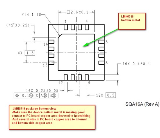
    Now my measurements are different from yesterday and there is quite some bias current flowing into/out of LMH6518. The chip is also quite warm at around 65C with a lot of air flowing. We did follow the recommendations regarding the pcb layout design but don't have quite the space in your evaluation board to implement a heatsink using the ground layers for LMH6518.

    The current flowing into -IN2 is ~13mA (way higher that the bias current in the datasheet) and current flowing out of IN1 is around 6mA! I am wondering if this LMH6518 is not damaged somehow.

    The base of T1 is now at -0.7V and the emitter is at -1.4V

    Alan

  • Hi Alan,

    The LMH6518 inputs should be around mid-supply (2.5V) if the schematic  you have attached works properly. The new emitter voltage of -1.4V makes sense, but there is still something wrong in that you are not getting the 2.5V (P9 voltage) you should be getting. That could possibly explain the LMH6518 heating up. I recommend that you first make sure your schematic portion is operational, before you hook it up to the LMH6518. You should get 2.5V at P8 and when you vary P1 (by varying your VG1 GEN), you should get a gain close to 1V/V at P8.

    With your circuit changed / corrected, please reattach the new node voltage readings.

    Regards,
    Hooman

  • Hi Hooman,

    The new node voltages with LMH6518 disconnected are attached.

    Alan

    LMH6518ScopeFrontEnd_LMH6518_disconnected.pdf
  • Hi Alan,

    Some comments:

    1. Please confirm that U2 output pin is close to -2.5V

    2. Please confirm that U1 inverting input is close to 0V. If U1 is operating properly (and there are no mis-connects), with P8 reading a low voltage, U1 inverting input would be lower than 0V, and that would cause U1 output to rise so that equilibrium is achieved. See if you can find out why U1 output is low and not rising (it could be that the R17, R18 are not what you think they are. Under equilibrium, R17 and R18 junction would be at 0V, but your situation you'll probably read something more negative (assuming U2 output is -2.5V, as it should be)

    3. Please confirm U1 and U2 supply voltages (Vcc= 5V, Vee= -5V)

    Let me know what you find out.

    Regards,

    Hooman

  • Hi Hooman,

    You hit the nail in the head with your first question! Somehow in software P7 was not set at 0V but -2.5V.

    After setting P7 to 0V the new measured values are pretty close to the simulation values (see attached pdf).

    I think a bigger than bias current flowing in/out of LMH6518 will happen when when the voltage at the input of LMH is bigger than 920mVpp (the recommended value). Could this be an explanation? Or it the chip actually damaged?

    I read in one of your previous threads here that the LMH doesn't have any protection diodes. What would be the right way to protect the LMH? If there is a need to protect it?

    The chip is still running pretty hot even when the input voltage is within 920mVpp - do you have an idea what temperature is running your eval board at?

    Thanks,

    Alan

    LMH6518ScopeFrontEnd_CorrectMeasurements.pdf
  • To be a little bit more clear - I think the differences between measurements and simulation were due to the fact the input voltage into LMH6518 was outside the 920mVpp valid range (because the vertical shift voltage at P7 was not set up properly) - would this be a fair reason?

  • Hi Alan,

    Here are some comments:

    1. LMH6518 temperature: Unfortunately I don't have a case temperature to report back to you. Have you verified that the 5V supply current draw matches the datasheet specification? The EVAL board for this device uses a 4 layer board with lots of vias for removing the die heat. This was brought up before on E2E:

    http://e2e.ti.com/support/amplifiers/high_speed_amplifiers/f/10/p/211919/749522.aspx#749522

    The PC board vias and PC board copper area are of utmost importance in keeping the die temperature low. Is your board done this way?

    2. LMH6518 input protection: You are correct in that there are no internal protection components. I don't think that your schematic original malfunction could have damaged the LMH6518. But, it is worth a try to bring up another PC board just to eliminate this as a possibility in your debugging efforts. The input protection has also come up before in E2E:

    http://e2e.ti.com/support/amplifiers/high_speed_amplifiers/f/10/t/252790.aspx

    Regards,

    Hooman

  • Hi Hooman,

    We did follow the recommendations for PowerPad design but I think we could increase the number of holes in the power pad area. We also don't have as much area available as you have on your development board. 

    Do you have the Tina-TI model for LMH6518 available?

    I searched for it on your website but could not find it.

    Thanks,

    Alan

  • Hi Alan,

    No, as you have already found out, unfortunately the LMH6518 does not have a TINA-TI model.

    Sorry.

    Regards,

    Hooman