This thread has been locked.

If you have a related question, please click the "Ask a related question" button in the top right corner. The newly created question will be automatically linked to this question.

LMH6554 Fully DC-Coupled Configuration with Shifted Dual Supplies

Other Parts Discussed in Thread: LMH6554, TINA-TI, ADS42LB69

Hi

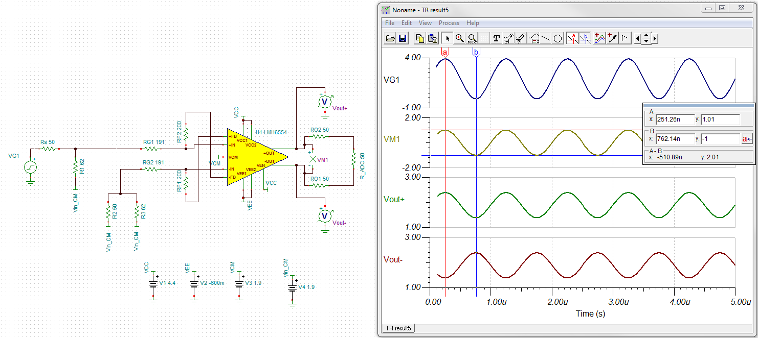
I would like to design dc coupled input configuration for LMH6554 with the following conditions.

May I ask if it will work? I am referring and simply change resistance values in Figure 6 on page 6 in Application report AN-2177 (SNOA565A). 

V+ 4.4V

V- -0.6V

Vocm 1.9V (=Vicm)

Vout 2Vpp

Ideally I would like to input 2Vpp(differential) or 4Vpp(single end) if LMH6554 can configured -6dB. 

In the AN-2177, Table 1 (Gain component Values for 50ohm System) on page 3 indicates minimum 0dB, if it cannot attenuate, then input voltage design can be 1Vpp(differential) or 2Vpp(single end) configuring LMH6554 gain 0db.

Also please advise if Rpu is required in Figure 6.  

Best regards,

Masa

  • Hi Masaharu,

    Inorder to maintain the input common mode voltage (Vicm) at 1.9V, it would be required to use the Rpu resistor as shown in the http://www.ti.com/lit/an/snoa565a/snoa565a.pdf when using V+ = 4.4V and V- = -0.6V. However, make sure that the Vicm pin swing in single-ended configuration is within +/-1.2V from either supply rails.

    Also, what is the DC input voltage of the signal source? Please make sure to include the DC input voltage of the signal souce when using the equation for calculating the Rpu. I have included the equation below for calculation of Rpu when Vicm = Vocm.

    It should be possible to use the LMH6554 as a -6dB attenuator. However, LMH6554 being a current feedback amplifier, make sure to increase Rg instead of reducing Rf for stability purposes. A minimum of Rf = 200ohms is recommended.

    Best Regards,

    Rohit

  • Hi Rohit,

    Thank you very much for your advices.

    I understand Rpu requirement. I will connect both +/- IN to V+ through Rpu.

    May I double check if the following configuration will work? 

    Vicm=1.9V 

    Vs=swing from -0.1V to 3.9V (single end 4Vpp)

    V+= +4.4V

    V-= -0.6V

    Vout (differential) = 2Vpp (-6dB gain result). Swing from 0.9V to 2.9V.

    Vocm=1.9V

    Does this work?

    About Vdcsource_cm(DC input voltage), is it voltage connected through Rt? If so, is it okay to use same V+(4.4V)?

    I referred equation (2) on page 6 in AN-2177. Is this as same as the equation you gave in your response? 

    Also may I have recommended Rg, Rt, Rm at -6dB? I am referring Table 1 on page 3 in AN-2177 and assume Rf=200ohms (can increase if need).  

    Thank you very much of your support.

    Masa

  • Hi Masa,

    It seems that your input swings 2Vpp centered at 1.9V dc (Vdcsource_cm) from 3.9V to -0.1V. So, I would think that you don't need the Rpu resistor.

    You only need the Rpu resistor when the Vdcsource_cm and output common mode voltages (Vocm) are different which happens to be the case in the application note AN-2177 with Vdcsource_cm = 0V and Vocm = 1.25V. In your case, the Vdcsource_cm equals Vocm to 1.9V and the Vicm will by default be set to 1.9V. However, one thing that you need to do is tie the Rt and Rm inputs to the same dc voltage as the Vdcsource_cm to maintain input voltage symmetry as shown in the below diagram.

    Following is the general equation which calculates what is the Vicm set to with your Vdcsource_cm and Vocm:

      where Rin = Rs||Rt + Rg

    For your case with Vdcsource_cm = Vocm = 1.9V, the Vicm will be equal to 1.9V (mid-supply) providing +/-1.3V room to swing for the Vicm pin. But, in the application note AN-2177, the Vdcsource_cm = 0V and Vocm =1.25V which set the Vicm to a different voltage other than 1.25V (mid-supply). Hence, there was the need of Rpu to maintian the Vicm close to 1.25V or mid-supply.

    To answer your questions, I think your circuit configuration of LMH6554 should work. Two things I noticed was that: 1. Connect the Rt and Rm to the same dc voltage as the source dc voltage (Vdcsource_cm) shown in the above diagram. 2. Inorder to get 2Vpp(diff) from a 4V(p-p) single ended input, you would need a 0dB gain in the LMH6554 because of the -6dB loss due to voltage division of Rs/ (Rs + (Rt||Rg)).

    "About Vdcsource_cm(DC input voltage), is it voltage connected through Rt? If so, is it okay to use same V+(4.4V)?"

    Ans: The voltage connected to Rt and Rm (where Rm = Rs||Rt) should be the same as the dc source voltage (Vdcsource_cm).

    "I referred equation (2) on page 6 in AN-2177. Is this as same as the equation you gave in your response?"

    Ans: It is a slightly different equation for Rpu which would end up giving you the same equation as in the AN-2177 if you set Vdcsource_cm = 0V and Vocm = Vicm. The AN-2177 document shows you how to set Vicm with Vdcsource_cm = 0V but depending upon application the Vdcsource_cm might be different than 0V, which you have to then consider in your calculation. In the below equation, the Vdcsource_cm is already 0V and if you set Vicm = Vocm, you end up with the formula Rpu = (V+ - Vicm)*Rin/Vicm.

    "Also may I have recommended Rg, Rt, Rm at -6dB? I am referring Table 1 on page 3 in AN-2177 and assume Rf=200ohms (can increase if need)."

    Ans: As I explained in my 2nd point above, you would need a 0dB gain in the LMH6554 because of the -6dB loss due to voltage division of Rs/ (Rs + (Rt||Rg)). I have attached TINA-TI simulation for your reference. I would choose the Rg, Rt and Rm to be the ones in Table 1 on page 3 in AN-2177 for 0dB gain.

    6758.LMH6554_schematic.TSC

    Best Regards,

    Rohit

  • Hi Masa,

    One last comment about increasing Rf is that the bandwidth of LMH6554 would decrease with increase in Rf because of the LMH6554 being a current feedback amplifier. I have attached a plot of bandwidth vs Rf which you could consider while choosing the Rf and the excel spreadsheet with the measurement.

    6013.4786.8524.LMH6554%20Freq%20Response%20for%20various%20RF6_14_12(1).xls

    Best Regards,

    Rohit

  • Hi Rohit,

    THANK YOU VERY MUCH for your professional support.

    I understand Rt and Rm connection to Vdcsource_cm instead of Rpu. 

    The TINA schematics and simulation you attached  is very helpful and I confirmed it on TINA.

    The LMH6554 BW vs. Rf ohm is very kind for further design change in case.

    Thank you again,

    Masa 

  • Hi Rohit,

    May I have another question about HD2 and HD3 simulation using TINA-TI?

    I use the TINA-TI scematics model you sent me in previous your response.

    I changed VG1 sine wave frequency to 25MHz and simulated Fourier Analysis as follows.

    I set Base Freq =25MHz and Format = (C*exp...). But I am not sure if this is Is the right way.  

    I got result HD2=1.99uV and HD3=510nV, then  calculated HD2 = -119dBc  and HD3 = -131dB as base amplitude (1.89V).  Is it right way and expected result in simulation?

    I am comparing this with Figure 13 on page 7 in LMH6554 datasheet. The simulation result is quite better than actual perfroamnce characteristics. 

    Best regards,

    Masa

  • Hi Masa,

    I think the fourier series simulation is correct. With the fourier series output format set to C*exp(j*(kwt + phi)), the first coefficient with k = 0 is the dc and if you calculate the fourier series expression for k=0, the output is 1.89 with phase set to 0degrees. However, this is not the fundamental output signal. The k = 1 is the fundamental output signal and the HD2 and HD3 must be calculated from this reference amplitude(C1). As a result, the HD2 and HD3 values come out to be 102dBc and 113.8dBc which is closer to Figure 13 on page 7 in the datasheet.

    Some things to note however is that the datasheet plots are specified with a gain of 2V/V which is different than the 0dB gain configuration you are planning on implementing. Also, the harmonics specially the HD2 will be highly dependent upon the layout of the board and matching of external resistors. To get very good distortion performance, I suggest to use 0.1% or better tolerance external resistors. The LMH6554 models for TINA-TI simulator are mainly derived from the datasheet and it is difficult to include matching or circuit parasitics thoroughly into the simulator. So, the simulation results will be better than the actual results to a certain degree.

    A suggestion could also be to characterize an LMH6554 evaluation board in the desired configuration and check true performance of the device.

  • Hi Rohit,

    Thank you very much for your answers and advices. Masa

  • Hi Rohit,

    I am changing the input signal swing = -2V to +2V and Vcm(Vdcsource_cm)=0V(GND) to save 1.9V offset volatge circuit (may require buffer amp with Vref). I added 2 x Rpu =160ohm caluculated with the eqution you previously provided (thank you it works). I am attaching TINA-TI scematics and simulated wave and got Fourier series Analysis with HD2=-103dBc and HD3=-113dBc.

    I would like to make sure if the final desig correct.

    2502.6758.LMH6554_schematic(Vdcsource_cm=0V).TSC

    And as a curiosity, I removed the 2x Rpu and analyze Fourier series with TINA-TI. I got degradation of HD2=-94dBc and HD3=-95dBc. I think that it is expected.

    Will get actual perfroamnce by EVM. The LMH6554 will be connected ADS42LB69.

    Best regards,

    Masa


  • Hi Masa,

    The final design looks good.

    Best Regards,

    Rohit

  • Hi Rohit,

    Thank you very much for all of your helps.

    Best regards,

    Masa