This thread has been locked.

If you have a related question, please click the "Ask a related question" button in the top right corner. The newly created question will be automatically linked to this question.

[PGA870] The output waveform level at the time of gain switching

Other Parts Discussed in Thread: PGA870

Hi,

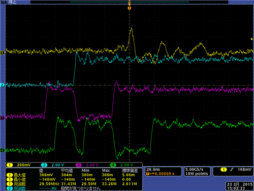
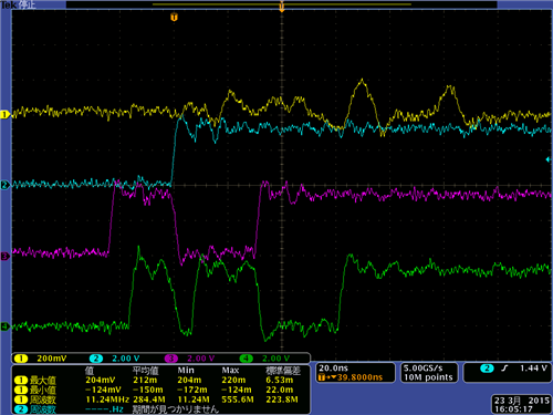
In case monitoring the output while switching the gain, the following waveform was observed.

 CH1:OUTPUT (However, this is not a PGA870 output.  through a buffer and gain amplifier)

 CH2:B5

 CH3:B4

 CH4:B3

The CH1 output is not PGA870 output , but even PGA870 output have the same behavior, so, CH1 will have considered equivalent to the output of the PGA870.

In most samples, in this situation, it is not only the half of the peak.

This situation means B5 is high and B4 transitions from Low to High and B3 transitions from High to Low at same time.

This is the other situation is not happening at the moment.

The first place do not stand only about 10nsec from B4 and B3 changes.

will things that should not be this time of data to measure?

In the data sheet, gain settling minimum time is 5nsec, I do not know whether it suffices to see how much the margin.

Input of PGA870 is no input, but I think what you fluctuates how much time you switch the gain as the output of the PGA870 that?

The IN + terminal I have GND connection with 75Ω of resistance to its destination with the capacitor of 0.1uF.

IN- terminal is connected to GND by capacitor of 0.1uF .

Is it possible to monitor the output in real time while switching the gain?

First of all, I would like to that point clear.

Thanks.

  • Hello Yoshida-san,

    For some reason I cannot view the attachment with the signal waveforms.  I am not sure, but it sounds like you are seeing the switching transients caused by the input offset voltage and the gain changes.  If you look on page 15 of the datasheet it shows that you can use the GAIN MODE and GAIN STROBE and LATCH MODE pins to have the gain change only when the GAIN STROBE pin changes logic level.  Otherwise there is a race condition between the parallel gain control bits where the gain of the amplifier is momentarily uncertain. 

    The reason that some amplifiers will have different behavior is that the input offset voltage is different and there will also be very small differences in the speed at which the gain switching circuits operate.  An amplifier with a large Vos and slow logic may have much larger output transients than an amplifier with small Vos and faster logic.  This kind of variation is normal.  This is the reason that there is the latched gain control mode. 

    Regards,

    Loren


  • Hi Loren,

    I'm sorry reply is too late.

    About story I got previous reply, I have questions.

    I was understanding about the possibility that the voltage peak generated at the time of gain switching by the offset.

    However, was measured by actual, larger device of the output voltage peak at the gain switching, the temperature change of the peak is large.

    If originally a small peak one, the temperature drift at 80 ℃ from 40 ℃  is about 10%, when the peak is larger, has increased by about 35%.

    And I seem to have a temperature dependent, but please tell me if you have any views on here.

    Figure1  The large peak

    Figure2 The normal peak

    CH1:Vout

    CH2:B5

    CH3:B4

    CH4:B4

    Thanks

    Tomoaki Yoshida.

  • Hi Loren,

    I have questions in addition.

    There is Gain settling time in the data sheet, but there is information only minimum time 5ns.

    How long time is maximum gain settling time?

    We are using single end output , using only out+ and out- is open.

    In this way we know it is vulnerable to common mode noise.

    However, voltage peak at this time of gain switching has confirmed that there is differential output.

    In this usage, do you believed that there is an influence?

    Since there is temperature dependent only larger peak one, is this a normal?

    I must think about how to avoid this if normal.

     Please comment  anything if.


    Thanks

    Tomoaki Yoshida.

  • Hello Yoshida-san,

    The gain setting time maximum is not guaranteed.  It looks like in Figures 10, 11 and 12 in the datasheet that the gain settings are all settled by 10ns but the plots are hard to read accurately.  I think that 20ns would be a safe number to use.

    Those voltage peaks look reasonable to me. 

    To the best of my knowledge this part was not ever tested using the configuration you are using, so it is very hard to say if the behavior is normal.  My opinion is that the measurements look reasonable for a single ended output response. 

     Have you considered using a transformer to convert the amplifier differential output to single ended?  Do you require DC coupling?

    Regards,

    Loren 

  • Hi Loren,

    I'm sorry not to be able to answer.

    A convert the amplifier differential output to single ended isn't used by our system.

    In our system, only OUT+ terminal is used.

    But a OUT- terminal has been just monitored, similar corrugation has gone out by reversed phase.

    So I think it can't be improved by a conversion differential output to  single ended.

    Isn't it good for this device to use single-ended output?


    In our system, it isn't necessary DC-coupling, and it is used AC-coupling.

    I think to lose a peak by a filter can consider, but is there a filter circuit of recommendation?


    Thanks

    Tomoaki Yoshida


     あなたは、増幅器差アウトプットを、終えられたシングルに変換するために変圧器を使用することを考慮したか? あなたはDC結合器を必要とするか?

  • Hi Loren,I'm sorry not to be able to answer.
    A convert the amplifier differential output to single ended isn't used by our system.
    In our system, only OUT+ terminal is used.
    But a OUT- terminal has been just monitored, similar corrugation has gone out by reversed phase.
    So I think it can't be improved by a conversion differential output to single ended.
    Isn't it good for this device to use single-ended output?
    In our system, it isn't necessary DC-coupling, and it is used AC-coupling.
    I think to lose a peak by a filter can consider, but is there a filter circuit of recommendation?
    ThanksTomoaki Yoshida
  • Hello Yoshida-san,

    This device was not designed for single ended output.  

    Even though a differential to single ended transformer won't entirely solve the issue it will help.  A transformer can also function as a filter, so if you can find a transformer that has similar bandwith to your signal it will also act as a filter for glitches.  That would be my first recommendation.

    If you send me your signal bandwidth I can suggest a filter.  Or if you want you can design your own filter using this software: www.aade.com/filter.htm

    Regards,

    Loren


  • Hello Loren,
    Because we can not be modified now circuit, it has stopped the time being considering the filter.
    I must investigate the cause of the bigger ringing at gain is changed.
    The small ringing ones will increase even about 10% at high temperatures, but the big ones also will increase 35% at high temperatures.
    I think so that there is a correlation clearly ringing volume and temperature dependent.
    About the cause of those ringing is large even worse at high temperatures, please tell me all the things that can be considered.
    Best regards,Tomoaki Yoshida
  • Hello Yoshida-san,

    Is it possible that you can attach the schematic or layout of the PGA870 circuit to help debug further? What are the supplies connected to and the supply current being read? Also, are you using the GAIN STROBE and LATCH MODE pins and what is the voltage levels of these pins when you are measuring the output waveform? Also, might be good to know what gain are you changing from and changing to? Looking at the output waveform, it does not seem that the gain is changing much.  When you are measuring the output waveforms on the oscilloscope, is it possible that you ground the probe on an adjacent signal ground and re-measure the output.

    Best Regards,

    Rohit

  • Hi Rohit,


    Thank you for your reply.

    I'm sorry, I can not paste the circuit diagrams and artwork here.

    Power of the PGA870 has been supplied with 5V from the power supply IC on the board.

    LATCH, RD_N and GAIN_STROBE pin are pulled up 1kΩ to 5V power supply line.

    And I had check these node dose not vary.

    Our problem is occured when B5 is high and B4 transitions from Low to High and B3 transitions from High to Low at same time.

    It does not happen in any other of the gain switching.

    In this case, large ringing occurs in the output voltage in some boards.

    I'mthinking  this ringing is not problem.

    Because there is also gain settling time, we understand that there are cases where some ringing caused by variations in the sample.

    Waveforms that were attached with more of the above is the actual output waveform of the small ringing  and the big one.

    However, I can not understand  that a large ringing sample is  increasing  ringing.

    Ta is 25deg the ringing  was 480mV , at 80 deg it was increasing to 650mV.

    A small ringing sample, 100mV does not so much change and 113mV.

    A large one is about 35% up, the small ones are about 10%.

    What are more reasons for ringing increases by large a temperature of ringing?

    If this is in the range of normal behavior, or that there is a temperature-dependent I want to know whether the abnormal state.

    We are for not standing pin to the adjacent GND, has taken the standards in GND terminal of the substrate.


    Best regards,

    Tomoaki Yoshida

  • Hello Yoshida-san,

    It seems that you are operating the PGA870 in "No latch" mode because the LATCH pins and GAIN_STROBE pins are pulled up to 5V. In this condition as Loren mentioned, the gain settling time would be dependent upon the race condition existing between the parallel pins (B5-B0).

    I would expect the gain settling time to increase with increase in temperature, because the supply current increases with temperature which causes the logic circuit to work faster. This means that in "No latch" condition, if propagation delay from B4 is lower than B3, the response of the gain transition logic would be to a higher gain until B3 logic propagates and thus causes the ringing in the output. I would think this is normal behavior, as dependent upon the process and temperature, the propagation paths for (B5 to B0) parallel pins would be different. As a result, I would highly recommend on using the LATCH and GAIN_STROBE pins for gain transition to get rid of any output ringing or overshoot.

    Best Regards,

    Rohit