This thread has been locked.

If you have a related question, please click the "Ask a related question" button in the top right corner. The newly created question will be automatically linked to this question.

LM7171 as a voltage follower; output voltage error

Other Parts Discussed in Thread: LM7171, THS4631

 Hello,

I am facing strange problem regarding voltage follower output.

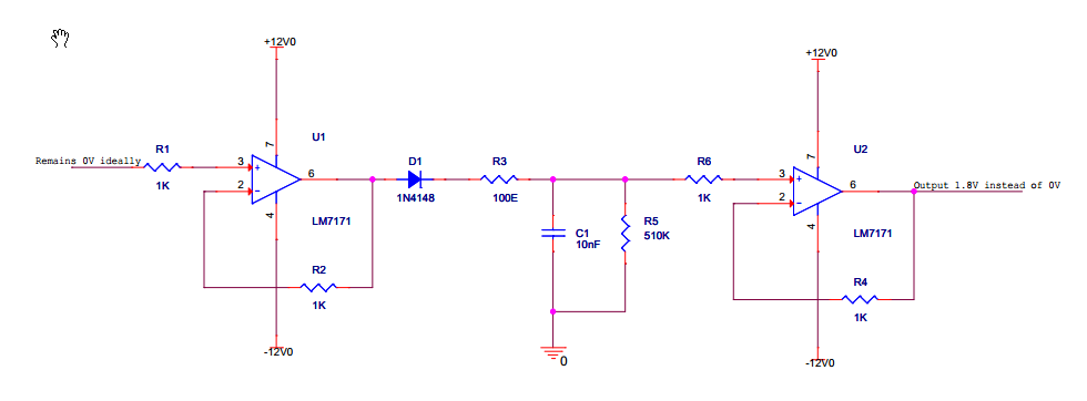
I am using LM7171 Op-Amp as a voltage follower with dual power supply that is +/-12V.

Description of circuit is as below:

This circuit is worked as a peak detector.

ideally my input signal at the first stage remains 80mV to -80mV. (almost 0V).

i have checked the output of U1( first stage voltage follower), it is ok. that is i get 80mV to -80mV. (almost 0V).

but if i check the output of final stage voltage follower U2, it shows 1.8V instead of nearly 0V.

ideally, when input signal remains 0V, then diode D1 will not conduct, & it will act as open circuit.

if op-amp's input terminal left floating, then output of op-amp will be uncertain.

So, i have pulled down non inverting terminal of U2 with R5 (510K).

if i have not pulled it down, then output of U2 will be saturated in positive side.

Now, the strange problem is here.

if i use 10K instead of 510K, then the output of U2, remains close to 0V. that is (150mV to 100mV).

when i increasing the value of R5, the output of U2 is also increasing.

Some practical result is as below:

100K       -     800mV

510K       -     1.8V

1M           -     2.4V

I can not use small value( less then 510K) for R5, as if i use small value of R5, capacitor C1 will be quickly discharged through it.

also i can not increase the value of C1, because number of signals for making peak is limited that is 500 signals.( in 500 signals , the out put of this circuit must show the peak value.)

i have also used decoupling capacitor at both power supply, as mentioned in the datasheet. ( these capacitors can't be seen in above circuit).

So, if i use 1M for R5, i will not able to detect peak which is less then 2.4V.

So, how can i solve this problem, without affecting peak detection accuracy.

Thanks in advance.

  • Hello,

    The 2nd stage (LM7171) input bias current (IB) is 10uA maximum. This current is supplied through R5.

    That is the reason you are seeing a large U2 output voltage with large R5.

    A high input impedance buffer between your peak detector cap and the input of the LM7171 would alleviate this, if practical? Choosing a lower input bias current part instead of the LM7171 (BJT input stage) would also help.

    On a different note, you are operating the LM7171 with a closed loop gain of 1V/V which may have some peaking in its response. The LM7171 minimum stable gain is rated at 2V/V. So, you may have to do some compensation to make sure your circuit is stable at this gain setting.

    Regards,

    Hooman

  • Hi Hooman,
    when input voltage is 0V, then diode D1 will be open circuit.
    Then how can R5 provide bias current to 2nd Stage voltage follower?
    I mean, R5 is pulled to ground, then how can it provide bias current?
    If this happen, how can i calculate R5 which is suitable for this application?
    you have said "A high input impedance buffer between your peak detector cap and the input of the LM7171 would alleviate this"
    So, which kind of buffer you want to say, i mean any voltage follower? or any other else?
    if voltage follower you want to say, then when input signal is 0V then,input of that
    voltage follower will be left floating & output of that buffer will be uncertain.
    i have selected this op amp because it has very high slew rate. is there any alternative of this part, then kindly suggest.
    when i use LM7171 as a voltage follower then which things should i care about?
    Thanks for your replay.
  • Hello JIGAR,
    All Op Amps need a DC path for the input bias current to flow, and in your circuit that is through R5. Think of the input bias current as the Base current of a BJT PNP flowing out of both input pins. The fact the other side of R5 is grounded is not an issue as you had noted.

    The error / voltage at the input due to this current is simply "R5 x i_bias". So, you can calculate what R5 needs to be for the amount of offset error that you can handle.

    A FET input Op Amp would allow to use a march larger R5 than a BJT input device. THS4631 can handle +/-12V supplies, and has 1,000 V/us slew rate (not as fast as the LM7171). Its maximum input bias current at 25C is 100pA (vs. 10uA for the LM7171). May be you can look it over and try it.

    Regards,
    Hooman
  • Hi Hooman,

    Thanks for the explanation.

    Now, i understand it.

    Ok, i will check FET input Op Amp.

    Thank you for your guidance.