This thread has been locked.

If you have a related question, please click the "Ask a related question" button in the top right corner. The newly created question will be automatically linked to this question.

TINA/Spice/OPA847: some questions about the peak on Frequency Response of a TIA based on OPA847

Part Number: OPA847
Other Parts Discussed in Thread: TINA-TI,

Tool/software: TINA-TI or Spice Models

Dear TI:

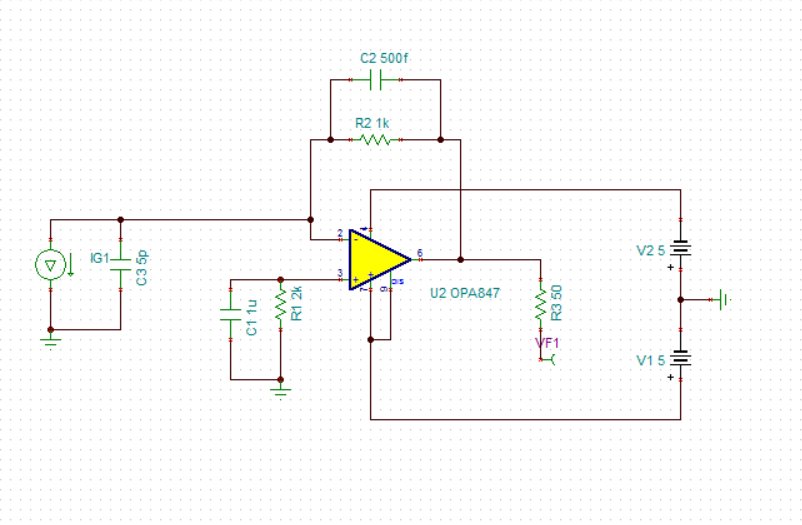
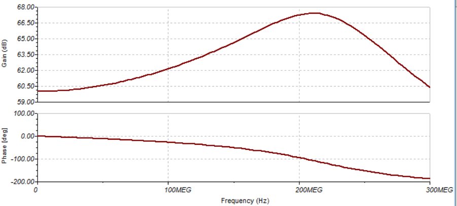
When I simulate a TIA based on OPA847 with TINA,on the frequency response curve,there is a peak on  200MHz .

I use a current source and a capacitor to imitate a PIN  Photo diode,5972 from hamamstsu.

so I have some questions about the peak

1.Why the peak could appear on the  frequency response curve?

2.How many components have the relationship with the peak?

3.How to confirm the frequency and amplitude of the peak?

Please give me some explanation about theory,

if you can give some  mathematical formulas,that is so good.

thank you very much


  • Xin,
    I am moving your inquiry to the High Speed Amplifier support forum.
    The experts in that product team will be better able to answer questions about your design.
    Regards,
    John
  • Xin,

    I am not sure why you are getting the response that you are. I hav e put you circuit into TINA-TI and I am unable to get the response. If youj can, please send me your simulation file so I can evaluate from here.

    In looking at your circuit there are a few things that you might want to change.

    1. Remove R2 from the cirucit. This resistor is not needed, yet it will create noise in your circuit. Ground the non-inverting input of the amplfier.
    2. Remove C3 from the circuit. This capacitor is also not needed, however it will have a profound effect on your circuit stability. Basically, in the evaluation of this photodiode circuit C3, C2, Cdm and Ccm add together to create the value of Cin.  Ground the non-inverting input of the amplfier.
      1. Cdm - amplifiers differetial input capacitance
      2. Ccm - amplifier common mond input capacitance
    3. Your closed loop signal gain is equal to R2 with a bandwidth of 1 / (2 x pi x Rf x C2)
    4. Your high frequency noise gain is equal to 1 + Cin / C2
    5. As you evaluate the gain and phase, I suggest that you look at the logrithmic frequency (instead of linear) response in Spice.
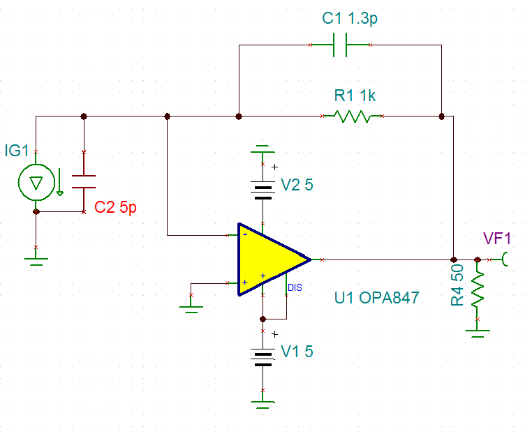
    6. Your selection of Cf is a little bit too low. I would recommend 1.3 pF to give you a 65 degree reponse which creates a circuit with approx 4.7% overshoot.

    The kind of circuit diagram that you should have is:

    You are correct in making the photodiode a capacitor and current source for your simulations.

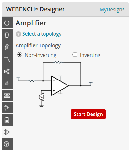
    You might consider a TI design site to do your circuit creation. I would recommend that you visit WEBENCH's Amplifier design site by clickin gon the op amp in the menu on the left. You will find this panel on the landing page of www.ti.com

    After you click on "Start Design" select the Photodiode (Transimpedance) Amplifier, Zero Reverse Bias.

    In the next view, Change the following

    Vref = Vout MIn to -2V 

    Vout Max to 2V

    TIA Bandwidth to 10 MHz

    Max Photodiode Current to 1 mA

    Click on "Create Amplifier Design"

    .You will find a list of amplifiers are shown on the screen. In the upper left corner of the table enter your OPA847 and you will see the sorting to that amplifier. To proceed on click on "Open Design".

    Good luck. Please get back to me if you have any other questions.

  • Hello Xin,

     The reason for the peaking is insufficient phase margin which in turn is a result of the amplifiers loop gain behavior. See the two part blog series below on how to stabilize TIAs for more information.

      One nuance to this particular situation is that the OPA847 is a decompensated amplifier, or in other words it is not stable in unity gain configuration. This means that the amplifiers non-dominant pole occurs before its open-loop gain (Aol) crosses 0 dB. This makes the analysis a little more complicated and there is no closed form equation to determine the amplifiers stability. What I usually do in such cases is plot the amplifiers Aol and noise gain and play around with moving poles and zeroes in order to get the correct response shape.

    In response to your question: what factors affect the shape; there are several factors (listed in the blog post) that affect loop gain and thus the frequency response shape.

    1. For example I can increase the feedback resistance from 1 kOhm to 3 kOhm (everything else stays the same) and consequently move the locations of the poles and zeroes and reduce the peaking.

    2. I can maintain the feedback resistance at 1kOhm and instead increase the feedback capacitance to 1pF and achieve a similar result with little to no peaking.(You should try this combination...for a frequency response with little peaking and still > 300 MHz closed loop bandwidth)

    -Samir