This thread has been locked.

If you have a related question, please click the "Ask a related question" button in the top right corner. The newly created question will be automatically linked to this question.

OPA656: OPA656

Part Number: OPA656
Other Parts Discussed in Thread: OPA659, OPA657, OPA857, TIDA-00978

I am trying to design a transimpedance amplifier circuit for visible light receiver operating at 400 MHz frequency. The circuits at high frequencies are effected by parasitic capacitance form bread boards.. Are there any PCBs with layouts designed specifically for OPA656 type amplifiers.

  • Hello Rakesh,

     Unfortunately, we currently don't have an evaluation module/PCB that can accommodate the amplifier AND photodiode. We however have a generic PCB for the OPA659 in a SOT-23 (DBV) package. Please see attached. I would recommend going with the DBV package since it is pin-compatible with the OPA657. What is the input capacitance of your photodiode? Also what is the transimpedance gain you require? These two parameters are important in determining if you can reach your 400 MHz bandwidth.

    EVM for SOT-23 (DBV):

    www.ti.com/.../DEM-OPA-SOT-1A

    Below are some articles on tranimpedance amplifier design:

    www.ti.com/.../sboa122.pdf

    e2e.ti.com/.../what-you-need-to-know-about-transimpedance-amplifiers-part-1

    -Samir

  • Thank you samir,

    The file attached below contains the design of TIA. 

    I may require a TIA gain of 3.3 k. Therefore the capacitance will be around 1.4 pF. The board you have suggested has some parasitic capacitance. So is it safe to choose the capacitor of much lower value?

    Also, how do I connect the photo diode(S10784) to this PCB? any suggestions?

  • Hello Rakesh,

    I have been doing some math and we currently don't have any amplifier that will meet your 400 MHz closed-loop bandwidth requirement. Even if I lower the gain and the photodiode capacitance I cannot find a solution. Are you absolutely sure you need 400 MHz of bandwidth? The photodiode you are using only has 250 MHz of bandwidth.

    Samir

  • 250 MHz is Ok for my application.
  • Rakesh,

     That may be possible with the LLMH6629. Please go through my posts and use the calculators provided to see how to configure it. I would also recommend using TINA to simulate your circuit. Another possible option is to use this deisgn.

    When you use the calculators, you may find that the photodiode you are using has very high capacitance which makes the design challenging. You may have to find a photodiode with lower capacitance.

    -Samir

  • I cannot chose other photodiode. For the SOT-23 you have suggested earlier, along with OPA656, what can be the maximum 3-dB bandwidth achievable? Why did you suggest OPA 857 or some other evaluation board?
  • With the OPA656 + 10pF diode + 3.3kOhm resistor the fastest you can get to is round 30 MHz. The OPA857 is a faster amplifier.
  • do i need a different evaluation board/PCB for OPA857? like TIDA-00978. I am looking for a cheaper PCB board.
  • You would need a different board for the OPA857...it has a completely different pin-out. Unfortunately, I do not have any cheaper boards to offer. You may have to design one yourself.

    -Samir
  • So, I will purchase OPA 857 and TIDA-00978. What about photodiode connection. In most experiments, the receivers have inbuilt TIA with photodiode. But I am using a special photodiode. How do I connect it to the PCB?
  • You will notice that there are 3 holes for a TO-Can photodiode. All the design files are available at the link below. Please go through them an ensure it works for you.

    www.ti.com/.../tida-00978

    -Samir

  • I have gone through the documentation of OPA 857. But I have some questions. Using the calculators posted in this forum, For a Rf of 3.3 K ohm and C diode of 10 pF, I get 181 MHz as approximate bandwidth.
    1) The TIDA evaluation board is intended to improve the bandwidth from 100 MHz to higher values. The calculations yield much higher than 100 MHz for OPA 857 for the same parameters(5 k ohm, 1.5 pF, GBW=6800 MHz). Why is this inconsistency?

    2) The datasheet of TIDA EVB shows Rf2 and Rf1 for 20 K and 5 K ohms respectively. Does it mean, there are only two possible gain levels? Doesn't external resistance effect TIA gain?

    3)I have referred to papers for VLC receiver(4.5 pF diode) using OPA 857 and they report the use of compensation capacitor which I think is the Cf/external capacitor in TIDA EVB lay out. With reference to www.ti.com/.../sboa055a.pdf
    I have found that 0.5 pF as external Cf can be chosen(Rf=3.3 K, CD=4.5 pF, GBW=6800 MHz) and the bandwidth of 256 MHz is obtained from calculations as F = sqrt(GBW/2*pi*CD*Rf). I wanted to verify this answer.

    I greatly appreciate if you can answer me how much 3-db bandwidth can be achievable with 5 pF diode, 3.3 k ohm gain using OPA 857 over TIDA.
  • Hello Rakesh,

    1. The bandwidth numbers that you see in the OPA857 are for 500mVpp signals which are no longer small signal so the calculators aren't going to be accurate here. You will notice in Figures 1 and 3 that the bandwidth numbers and peaking change a lot with a change in output load. This is again the result of large signal effects on the amplifier output stage.

    2. The labels of 5kOhm and 20kOhm only indicate what resistance setting is chosen inside the amplifier. The OPA857 doesn't just change the feedback resistance when you change from 5kOhm to 20kOhm. It also changes the feedback capacitance (Cf) and more importantly it also changes and more importantly it also changes the amplifiers internal compensation so that the amplifier actually has more GBP @ 20kOhm vs 5 kOhm.

    3. Unfortunately the TINA SPICE model for this is not very accurate so its hard for me to give you a bandwidth number here. You will have to evaluate this yourself in the lab with the actual board.

    -Samir

  • Thank you for answering my questions.
    So, by using the TIDA EVB and OPA 857, I could avail only two possible gains either 5K or 20 K.
    The external Rf and CF are fixed and soldered on the EVB, so I cannot change them.
    All I know is the photodiode capacitance is 4.5 pF. 130 MHz is achievable for a generic OPA857 with 5 K gain and 1.5 pF. If the capacitance is higher (4.5pF+stray), i will get far lower than 130 MHz. Does the design for TIDA EVB can improve it?I totally understand that accurate measure cannot be obtained by simulation ,but I would like to know the worst case bandwidth/least that i can get? I cannot invest on this component and EVB if the bandwidth is too low.
  • The external Rf and Cf are components soldered on to the board. You can change them to any value that you prefer if you have a soldering iron.

    5k and 20k are the internal resistors. Those values are fixed. The jumpers on the board allow you to select either gain setting and then in conjunction with the external resistor you can vary the effective transimpedance gain.

    The SPICE simulation is pessimistic, so since you are looking at worse case scenario and using the following conditions:
    1. Internal transimpedance gain = 20 kOhm
    2. External Rf = 3.3kOhm
    3. External Cf = 0.2pF
    4. Diode capacitance = 5pF

    Output -3dB bandwidth = 250 MHz (worst case)

    -Samir
  • Ok,
    I can go with 200 MHz as well, so not a problem even in worst case scenario.
    The Photo diode, I am using has two terminals(Not a TO-Can), Can I leave the third terminal/hole on the board as is.
    I have to buy TIDA EVB and OPA 857 seperately. Right?
  • Yes, you can leave the 3rd terminal unconnected.

    The TIDA-00978 board comes with an OPA857 on it. If you need a few extra you can order them at estore.ti.com

    -Samir
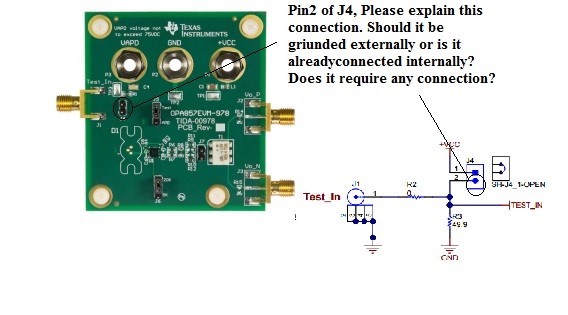
  • Hi, I have few questions regarding the connections on the TIDA-00978 EVB. Kindly answer them.

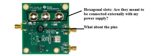
    Q1. Connection of hexagonal slots?

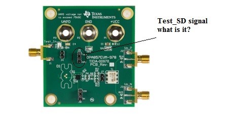
    Q2. Test_SD signal what is it?

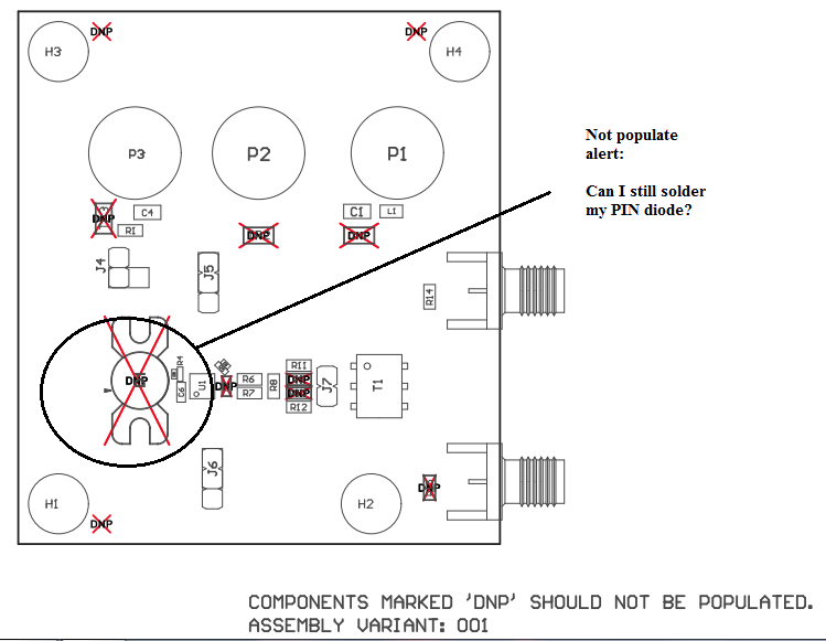
    Q3. Do not populate alert on PCB. What about my own photdiode?

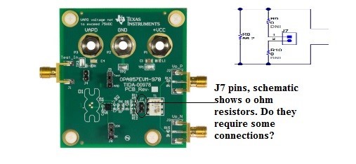
    Q4. Connecting J7 pins? Schematic shows zero ohm resistors

    Q5. Pin 2 in Test_In or near J4

  • Q1. Connection of hexagonal slots? : Yes that is for Power and GND as well as photodiode power.

    Q2. Test_SD signal what is it?: That is test mode. Please read the datasheet to learn how to use it or disable it.

    Q3. Do not populate alert on PCB. What about my own photdiode?: Yes you can populate your own photodiode there.

    Q4. Connecting J7 pins? Schematic shows zero ohm resistors: That is your choice depending on how you want to connect your scope.

    Q5. Pin 2 in Test_In or near J4: Again this is for test mode..please read the datasheet.
  • Thank you. I have not used EVB before. Could you please tell me what kind of connectors are used for the hexagonal slots?
  • Hello,
    Those are banana jacks. I would highly recommend getting help from someone in your lab who has more experience with test and lab equipment and setups.
    -Samir
  • Hi,
    I still cannot figure out the connections at J4. I have connected the PIN 1 of J4 to Vcc and left PIN2 open and found no signal. Also tried Pin1 Vcc and Pin2 Ground, still no signal at the output. This port is the interface between the amplifier and the input test signal.
    I have set the bias to 2 volts and I found the same DC volatge at pin2, which means the signal is entering the EVB, But the output of EVB on oscilloscope does not show my input trace at all. Multimeter does not show any reading.

    I can skip the test_mode and proceed with soldering a photodiode. I should know some way to check if the EVB is working fine.

    I cannot identify where the problem is, despite testing it several times as per the instructions on the data sheet(test_mode).
    Kindly refer to my question on TIDA 00978 in TI design forums and help me identify the problem.
  • To test the amplifier in test mode -

    1. set the Test_SD pin to +VS .

    2. Set a dc voltage on the test_in pin (J1) to around 1.9V using a dc input and sweep the voltage up to around 2.4V. Make sure the J4 jumper is disconnected when doing this otherwise you are going to just short J1 to Vcc.

    3. As you sweep the dc voltage on test_in measure the amplifier output on the left side of R6. Once you see the output start to move you can figure out the transfer function of Test_In input voltage to OutP, output voltage.

    4. The test procedure in section 5.1 of the TIDA-00978 user guide actually goes through it. If you could have someone in your lab with good lab skills you should lean on them for help. We have had many people use this device in test mode and not had so much trouble as you are having. Please lean on someone with good electrical engineering and lab skills to help you out.

  • Thank you for the reply.

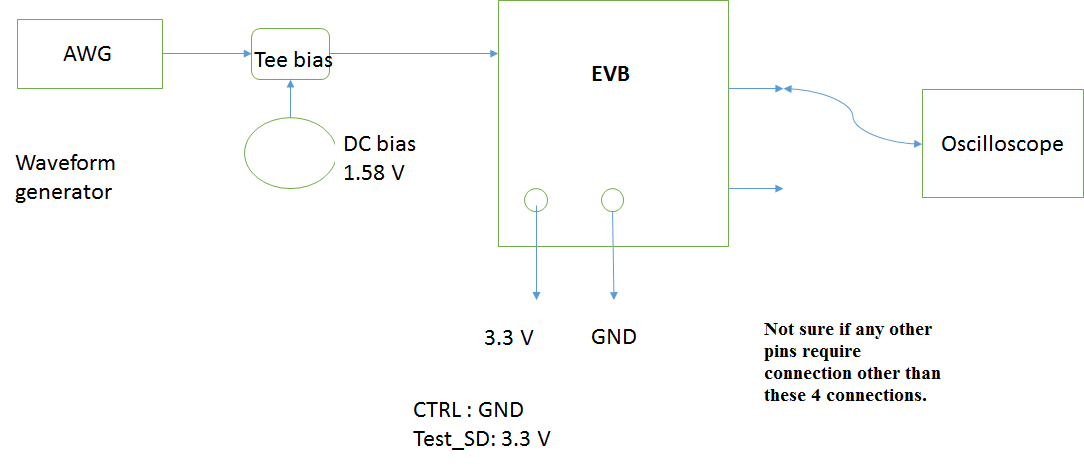
    I have tested the board as given in the reference. I have gone through the section 5.1 and followed the procedure. Using figure 3, I have made the connections and also based on the steps in 5.1. My device set up is shown in the figure below. I have never seen any output which is atleast close to the input frequency. I do not know if this the correct way to set up using a tee-bias.

    I have used TI EVBs before and my major is electrical engineering. If there is any fault within the board, there is no simple way to check it.It must need some indicator/test. 

  • What is the quiescent current that the device is drawing in normal mode?(21 -25mA)

    What is the output at OUTP in normal mode?(1.83V)

    What is the output at OUTN in normal mode? (1.83V)

    The above are very basic initial tests to perform to check for basic functionality. The indicators for checking if a part is working usually needs some debug effort and knowledge of the datasheet.

    In test mode, why don't you just start with basic DC testing instead of trying with a sine wave? DC testing is generally considered easier than AC testing.