This thread has been locked.

If you have a related question, please click the "Ask a related question" button in the top right corner. The newly created question will be automatically linked to this question.

TRF37D73: Amplifier output spur

Part Number: TRF37D73

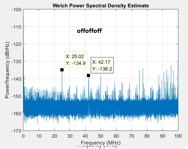
I built a three stage amplifier using TI's general purpuse amplifier block TRF37D73, the schem is just like the reference design. The frequency range is from 8MHZ to 68 MHZ, I put a bandpass filter in the output end. I tested it and found there are some weak interference spur in it's output port. Please see the figure attached. Does anyone can tell m e how to eliminate those interference?

  • Hi Duan,

    Are you terminating the input with 50-ohms and measuring the spectrum? Is there enough power supply de-coupling present on the TRF37D73 supplies? 

    Cascading a 20-dB RF amplifier in three stages could introduce a lot of spurs, especially at lower frequencies, if proper supply de-coupling is not present. I would recommend a 0.1uF ceramic cap on each of the TRF37D73 supplies in-addition to a 1uF tantalum on the main supply. Ferrite beads to isolate the stage supplies would also be recommended. Also, care should be taken not to route the input and output signal traces close to each other. 

    It would greatly help if you could provide the schematic and layout diagram of your test circuit to further help debug the issue.

    Best Regards,

    Rohit

  • Hi, Rohit;

    THX for your reply.

    Yes, I did put a 50 ohm terminator in the input.

    following in my schematic:

    all the three stage are same. I put two SPDT switch before and after the TRF37D73 so I can bypass it. To clarify the multi-stage coupling effect, I turn on only one stage, and other two are pwdn and bypass, following is the results:

    you can see the spurs still exist even I turn one stage, but the spur frequency is different.

    to compare the three stages are all turn on:

    following is the time domain:

    you can see the periodic spikes that is the interference.

    also, following is my PCB layout:

    that a 6 layers PCB. To let you see the detail, I zoom in one of the three stages:

    PLEASE HELP ME!

    Donald

  • Hi Donald,

    I think the schematic looks okay. Is it possible to bypass all the three TRF37D73 devices and see if the interference spurs exist, or basically do an OFF OFF OFF condition? Also would it be possible to provide BOM info on the RF choke inductor?

    Something you can also try is playing around with the RF choke inductor from 1uH to 4.7uH or 100nH and see if the interference spurs go away. You could also try an experiment of including some series resistor of 5ohm to 10ohm at the TRF37D73 output. For starting purposes, replace the C14 with a 5 or 10 ohm resistor and see if the interference spurs reduce. I think the RF switch is AC coupled on the common input, so it should be okay.

    I think the bigger problem here is the layout where you are routing single-ended signals over long PCB traces, which is very much susceptible to common mode noise or interference. One way to avoid this is by isolating the individual stage supply VCC and GND from each other. You could then connect those together using ferrite beads on the top layer. Also, it looks like the supply bypassing cap for the TRF37D73 is on the bottom layer and not right next to the device on the top layer, which is something I would avoid. 

    Best Regards,

    Rohit

  • Hi, Rohit;

    THX for your seggestions and I will try next week.

    The choke inductor is MURATA's bead BLM18EG471SN1, its characteristic is as following:

    Thanks again!

    Donald

  • Hi, Rohit;

    Sorry for the delay, I was on a business trip and back to the office today.

    We baught a TRF37D73 EVM and tested it:

    You can see the spurs are below -142dB, the signal at 42.17MHZ should be the interference out because we were not tested it in a shielding room.

    Then the result of our amplifier in offoffoff state:

    we can see the spurs are also at around -145dB.

    And if we turn on the third stage amplifier:

    in this case we think maybe the spurs are due to our layout and we arre going to re-layout our PCB. Chould please send me your EVM PCB layout so we can follow?

    THX!

    Donald

  • Sorry! I found the PCB layout of EVM in the document of the EVM. We will re-layout a PCB and let you know the result.
    THX!

    Donald
  • No Problem Donald.

    Best Regards,
    Rohit