This thread has been locked.

If you have a related question, please click the "Ask a related question" button in the top right corner. The newly created question will be automatically linked to this question.

THS6002: THS6002 Output Issues

Part Number: THS6002
Other Parts Discussed in Thread: LMH6739, THS3092, THS6012EVM, THS6012, THS3001, THS3096

My customer is seeing the following issues with the THS6002:

I'm using this part for its high-speed/bandwidth current FB capabilities, but not for an ADSL application. I targeted this part for its "quad" packaging as I need 64-channels of analog output in a minimum footprint. I also ran several p-spice sims to evaluate various parts for this challenging application.

After implementing the design, I'm seeing strange "recovery" type behaviors which are triggered by full-scale negative going steps (only) that are followed by an approximate 2 usec period of random reduced amplitude output.  The part exhibits no problem with similar full-scale positive edge step responses.

I am using the parts (trying) to create a uni-polar 0-to-12V output with a small (hi-Z) load. I'm running them with a 1.2K FB resistor in a  6 gain configuration to achieve a 12V output from a 2V p-p input. The worst case signal input is effectively a 25 MHz square wave from a DAC running at 25 MHz clock rate.

Thinking the "negative only" behavior was perhaps a supply headroom issue, I increased the negative supply rail as far as -15V (initially designed for  15/-5V). The increased supply headroom has no affect on the strange behavior.

The 0-2V input waveform has some ringing (overshoot/undershoot) and a fast rise/fall time of approximately 2 nsec.

Is this asymmetrical behavior possibly due to some kind of internal saturation issue specific to the THS6002 device?  What can I do to correct it?

Unfortunately, the circuitry is at my clients facility and I did not think to capture any scope trace pictures earlier that I can send you. It will be next week before I can do that.

I have attached schematics of both the source signal buffers and the amplifier circuits annotated with notes.  I realize the whole configuration is far from ideal, but its what I was given (as a design consultant) to make system “speed improvements” on.  I have provided a re-design of the video buffer cards as well as new amplifier cards that are arranged in two-card stacks with ribbon cable interconnects.  Each card contains 32-channels of signal amplification.

Both the buffer and amplifier pcbs are 8-layer with all input/output signal traces on controlled impedance internal layers (stripline) between ground and power plane layers. In a rush to get the pcbs finished, I did not take the time to add plane layer cutouts around the amp input pins to minimize capacitance.  Since the components were so close and traces so short, I gambled that wouldn’t be necessary. 

Also, prior debug steps have included:

Temporary increase of decoupling (handheld on amp pins) – no observable changes noted.

Reduced FB resistor values (and gain) slightly – no improvement, actually made erratic response worse.

Maximized power supply headroom – no improvements noted.

Added stray capacitance on input pins (via fingers etc) – no observable changes noted.

The amp behavior doesn’t really look like an instability since its only associated with negative transitions? I would think a phase induced oscillation would be present all the time, instead of just on negative step responses?  I have since noticed in the datasheet the 70ns “settling time” for 01%, and some rather low BW numbers for “full power” operation. Even these do not explain a 2 usec recovery time after a full-scale negative transition.

I have attached his schematics.

THS6002 Output Issues_THS6002 Amp Sch.pdf

THS6002 Output Issues_Video Buffer Input Sch.pdf

My question is whether he can set up a gain of 6 and still be able to meet the specifications in the data sheet. The only references to gain that are given are either 1x or 2x. Is he having a bandwidth issue when the fast negative signal appears on the input? The recovery time also seems odd, but there is nothing specified in the data sheet regarding the recovery from an over-voltage situation. He is driving the outputs near to the rail.

I am sorry I cannot provide a scope shot of this behavior right now, but I hoped that you might be able to diagnose the problem by just seeing the schematics and an explanation of the circuit.

Please let me know if you have additional questions for the customer.

Thanks for your help with this!

Richard Elmquist

  • I have further information from the  customer:

    I did manage to capture some scope traces this afternoon.  As you can imagine, the behavior was extremely difficult to trigger the scope on and capture a stable trace. Since the amp outputs aren’t perfectly repeatable, most traces just look like random garbage.  But I’ve put together some slides with annotations pointing out and answering some of your questions hopefully.

    THS6002 scope.pdf

     The “negative” edges I was referring to aren’t negative voltage. I just meant (digitally speaking) falling edges or “negative going”.  The op-amp inputs are 0-2Vp while the needed outputs are 0-12Vp.  I’m hoping the designed power rails of +14V and –5V provide enough headroom to prevent saturation from that perspective.  I have temporarily increased the negative supply to –14V (as a check) and that made no change or improvement in the amplifier’s outputs.

     I have also discovered a different test image that improved the DC offset a bit (between true/inverse image periods) such that both falling and rising edge steps were a bit closer to “full-scale”. That image managed to break the amps output all the time.  In that case (sorry I didn’t capture a pic), the amps were recognizably trying to produce the “ramp” signal waveforms, but with reduced effective gain.  In other words, the signal output was only swinging between 3-4V on the low side and 8-9V on the high side.  The slew rate was still plenty fast, just lost amplitudes. Not sure I would recognize that as a BW issue, but there’s obviously some amp limitation.

     Bottom line question for your designers – is the THS6002 capable of doing this?  I chose it based on seemingly adequate BW specs in the datasheet, before noticing the relatively pathetic “full power BW” numbers in the details.  If this is not the correct part, what would your recommendation be to achieve this pipe-dream? 

    This looks to me like the op amp is saturating and then takes a while to recover. I have asked him to increase Vcc to +/- 15V and see if this has any effect. I believe that this might also be a byproduct of not enough bandwidth as the customer asks.

    Please let me know what you think. Let me know if you have any further questions for the customer.

    Thanks for your help with this!

    Richard Elmquist

  • Hi Richard,

    To answer your questions in the first post, it is possible to set up the THS6002 for a gain of +6 and still be able to meet the specifications in the data-sheet. If you look at Figure 30 and Figure 51 in the datasheet, they both give the pulse response for G=+5 with Vo = 20Vpp at tr/f = 5nsec.

    Regarding the recovery scenario, the min output voltage swing tested on +/-15V supply is from +11.8V to -11.5V (see page 4 in the datasheet). If the THS6002 output swing is from 0V to 12V in the customer's application, I don't think this is a hard enough saturation. In such a scenario, the recovery from this saturation should be quick for both the positive and negative going input transitions. One way of quickly verifying that it is indeed the saturation that is causing the issue is by increasing the positive supply voltage. Would it be possible for the customer to increase the positive supply voltage to say +17V or +20V keeping the negative supply voltage at -5V and see if the issue goes away?

    To answer your questions in the second post, it is possible that the THS6002 does not have sufficient bandwidth as the customer mentions. However, the reduced BW would show up for the positive transition as well. So, I am not quite sure whether the reduced BW could really relate to the negative transition issue that the customer sees. One possibility of increasing the BW is by reducing the Rf value to 680 ohms and accordingly scale the Rg to 136 ohms for G=+6 to see if the Trise/fall of the output transition decreases.

    It also seems that the LMH6739 outputs directly drive a ribbon cable interface via 73-ohm pcb stripline and then connect to the THS6002 input. Usually, ribbon cables are notorious for doubling the source voltage due to signal reflections if there is not adequate source termination. As a result, would it be possible to include some series resistance (on the order of 30ohms to 73ohms) at the LMH6379 output to make sure there are no signal reflections at its output? You could try scaling the THS6002 gain accordingly to compensate the loss in those series resistors at the LMH6379 output.

    Best Regards,

    Rohit

  • Rohit,

    Thanks for your response!

    I will send your comments to the customer and will let you know if this fixes the issue.

    Thanks again.

    Richard Elmquist

  • Rohit,

    Here are some further scope shots once the customer has expanded the supply voltage to +/- 15V.

    THS6002 scope2.pdf

     Here are the customer’s comments:

    Here’s some scope pics of today’s testing results.  I re-wired the THS6002 amps directly to the system’s +/-15V power supplies. The amplifiers seemed to behave a small bit better in that the problem responses were more stable/periodic and it was easier to trigger the scope and capture repetitive traces.  Otherwise, the increased supply headroom did not have a dramatic effect.

     Some of the zoomed in scope pics reveal what looks more like a BW issue when the amp is not responding to the small incremental waveform steps during the “recovery” periods either. The small stair-steps look to be filtered into a smooth ramp response.  But again this is only after a large falling edge step!

     Hopefully your factory engineer can make some sense out of this.  I left a tech today attempting to haywire a “filter” on a few of the LMH6739 inputs to try and get rid of some of the high frequency ringing out of them. I also received some components today for setting up some individual part breadboards to more conveniently play with gains and such. It will be next week before I can report much in results from these efforts.

     Question – is it possible that parasitic pcb capacitance on the THS6002 input pins could be causing this type of behavior?

     Could it be that the supply voltage was still not high enough?

     Could the trace capacitance possibly be causing the issue?

     Or does this appear to be a BW issue?

     Thanks for your help with this!

    Richard Elmquist
  • Rohit,

    The customer has done some further testing and the results are shown in the attached file;

    THS6002_scope_3.pdf

    Here are his comments on this:

    I have re-created the THS6002 circuit on a breadboard setup that allows somewhat easier tweaking.  The chip is on an SOIC-to-DIP adapter pcb with pins plugged into an old (classic) breadboard and components plugged in as close as possible. I’m not sure the parasitics are much better, but they are at least different!

    I managed to accidentally capture the amp doing something similar to my production pcb, but surprisingly it was triggered by varying the input signal amplitude!  The attached charts capture an entire sequence of scope pics showing the circuit response to inputs from 0-1Vp up to 0-2.1Vp.  The amp behaved reasonably up to around 1.5Vp when it started saturating/oscillating similar to before.  Increasing the input to 1.8V stabilized the response, but the output amplitude was greatly reduced and with a positive offset.  Bumping the input up to around 2.1Vp seemed to snap the amp out of its reduced amplitude mode and almost back to expected levels but still with a small positive offset.

    What is going on??   Insights from the factory experts will be appreciated.

    I can do another pcb layout to improve parasitics or decoupling, etc., if that’s the issue. But if this behavior is due to a part limitation I need to know soon so I can pursue a different amplifier component.  Perhaps the THS3092 can do a better job for this application?

    He has increased the supply voltage to +/-15V. I am going to suggest that he increase it even higher.

    Do you have any idea of what is causing this? I can understand the loss of amplitude if the op amp cannot gain up the signal properly, but it seems from his test that it varies and that an offset is also seen. Can you reproduce this? Would the THS3092 possibly be a better option?

    Please let me know if you have any further questions for the customer.

    Thanks for your help with this!

    Richard Elmquist
  • Hi Richard,

    Let me take a look and get back with a reply or alternative soon.

    Best Regards,
    Rohit
  • Hi Richard,

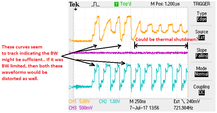
    Looking at the scope capture waveforms in THS6002_scope2 pdf file, it is possible that the fast falling edge issue seen at the THS6002 output could be related to the internal thermal shutdown of the part. In the Applications Section of the THS6002 datasheet, it is mentioned that the part has a built-in thermal shutdown protection feature if the internal junction temperature rises above 180'C. Does the customer have any heat-sink on the part that dissipates heat out of the package, or is it only the bottom thermal pad that conducts the heat? If there is no heat-sink on the part, I would try the below experiment with a heat-sink to see if the issue goes away.

    I think the issue is more related to thermal shut-down rather than BW because if I look at the below scope capture, the two input and output waveform cycles track each other somewhat. However, the waveform in-between them and subsequently after the second good waveform, it seems the THS6002 goes into an unknown state indicating the part could be turned-off until the internal junction temperature cools down. Also if it was BW limited, I would expect both the two good waveforms to be distorted as well. In addition to that, it seems one channel worked good based upon the comments in THS6002 scope pdf file.

    For increasing the supplies to +/-15V, I don't think this scenario is any different than the +15V & -5V supply because the output really does not go down to the negative rail. A better experiment would be is to make the THS6002 supply as +20V & -5V which will eliminate any possibility of the output saturation that couples with the customer's issue. However, since the thermal shutdown still exists with +20V & -5V supply case, the customer should still see the distorted waveform indicating thermal shutdown to be the main culprit.

    I think going forward in the next design, it would be better to switch to THS3092 because there are lesser devices per package which will help in keeping the internal junction temperature lower. Also, it has higher large signal BW compared to the THS6002 which will make the rise/fall edges sharper. However, before switching to the THS3092, I would still perform the heat sink experiment on the existing board to make sure it is indeed the thermal shutdown that's causing the problem. The customer could also try powering on only one out of the eight devices to see if the board heating is causing any trouble.

    Best Regards,

    Rohit

  • Rohit,

    Thanks for your response!

    I has not thought of the thermal effect. This could be the issue.

    I will have the customer try the tests that you recommend and I will let you know if he has any further questions.

    Thanks for your help!

    Richard Elmquist

  • Rohit,

    Please see the customer’s comments below:

    I’m having difficulty believing the behavior is due to thermal shutdown due to actual thermal issues.  On my production pcb’s the parts are well heats inked through the “power pad” on the bottom and soldered to two internal ground planes.  As a result the parts get a bit warm to the touch and the pcb warms up globally as well indicating that the thermal pads are working. There are no additional heat sinks on the top of the packages as it doesn’t seem necessary.  The parts only get a bit warm to the touch (I guess around 40C) so I can’t imagine the junction temperatures are anything close to 180C!  Perhaps the thermal shutdown circuitry is sensitive to power supply noise or something else?

    On my breadboard, I have increased the supply rails to both  +17/- 17V as well as +20/-10V with no effect on the output response.  No headroom issues evident.

    I’ve also varies the waveform frequency several magnitudes.  The output looks good at really slow (10KHz range) but then it has plenty of time to “recover” from any edge.  When the frequency gets close to 1MHz it starts exhibiting problems all the way to 20MHz (which is the max range on my signal generator).  The response varies a bit over the range, but so does the input waveform due to reflections.  I think the main effect of frequency is slight variation of amplitudes/reflections on the input.

    Doesn't sound like the factory engineer has seen or responded specifically to the last set of pics I sent you showing the input amplitude sensitivity??  I would be very interested in their take on that.

    I have suggested that he try the THS3092 since he is bread boarding this, It seems to me that the bread board could be causing some of the issue that he is seeing. Can you look at the comments and let me know if you have any additional questions or comments?

    Thanks for your help with this!

    Richard Elmquist
  • Rohit,

    Here are some further comments from the customer about this issue.

    On my pcb’s I have no practical way to selectively power off some of the amps.  It’s all or none unfortunately. We had played with some “cold spray” on some of them and “freezing” them did have some effect on the output waveforms, but did not “fix” the shutdown looking issue.

    My breadboard chip does get much warmer since it is not connected to any heatsink. As a result, I have been limiting its operation to a few minutes at a time.

    I did procure a TI eval board for the THS3092 in preparation for having to proceed with a potential re-design. I can power that up and check its operation for this application.

    Meanwhile, I will continue to play with the breadboard THS6002 chip to see if I can discover any other correlations to the behavior other than signal amplitude shown in the “THS6002_scope_3” file.

    Please let me know if you have any further replies that I can send to the customer.

    Thanks for your help with this!

    Richard Elmquist

  • Hi Richard,

    Sorry for the delayed response.

    For a high speed/high voltage part like the THS6002 or THS3092, I would not recommend putting the device on a bread-board because you might end up with un-expected results due to board parasitic. The electrical connections are also loose and there is no connection to the thermal-pad which in-turn brings the thermal shutdown into question. Instead, I would recommend using the THS6012EVM which could be used to evaluate the THS6002 device.

    Regarding the customer's comments about thermal shutdown, is it possible to verify the actual temperature on the THS6002 part using an IR Camera? If the parts get a bit warm to touch and the pcb heats up globally, then it means that the part's internal junction temperature is also high and the thermal pad underneath the part is not sufficient to remove the heat out of the part. Do you happen to know what effect did the cold spray have on the output waveforms? Did the output waveforms happen to stay on for a longer time? It is possible that the thermal shutdown circuitry is sensitive to power supply noise where there is some charge injected into the circuit to turn it on for higher frequencies.

    I think it would be better to switch to THS3092 for future designs because of higher large signal BW and lesser devices per package compared to the THS6002.

    Best Regards,

    Rohit

  • Rohit,

    I sent the customer your response. I also was very leery about using this device on a breadboard and told him so.

    Here are some further comments from the customer:

    I essentially disabled the D1/R1 amps by tying their inputs to GND. The output of the remaining two D2/R2 amps cleaned up and looked good with the previously problematic 0-1.6V input amplitude. This might support the thermal shutdown theory due to the relatively slow response of the recovery periods (in the 1-2usec range), except for the fact that the part package is not getting that warm.  Since I have no insight into how the shutdown circuitry is implemented, it also seems odd to me that the output amplitude swing is reduced to half and is centered about the midpoint of the “correct” output signal swing as if there is an AC-coupled gain stage somewhere?

    Second, with half the amps operating at null input, I increased the input amplitude back up to 0-2.1Vp and the problem began re-appearing on the remaining two amps. Again the oscillating periods of reduced gain followed by return to normal in 1-2 us.  I increased the power supply a bit to run at +20V/-5V to test for any headroom issues and found none.  I also played with the input signal offset to better center it about GND reference. The output followed the offset up and down as expected, but still exhibited the “shutdown” periods of reduced gain/swing amplitudes.

    Third, I swapped in a lower feedback/gain resistor values on R2 amp to 820 ohms (with 160 to GND to maintain the A=6 gain). The output waveforms improved a bit (with cleaner sharper edges) but the shutdown oscillations were still present and readily observable with input signal amplitudes increased further to around 0-2.2V peak.  Starting to sound more like an input stage saturation effect precipitated by the larger input signal swing amplitudes?

    Question 1 – is it possible that parasitic coupling between +/- amp input pins could induce this “slow” oscillation effect?  I would think this kind of instability would be of a much higher frequency given the parts normal BW and slew rates.

    Question 2 – Is it possible that there is excessive internal coupling when all four amps are running simultaneously with the same input signal to create a saturation effect?

    Thanks again.  I need to focus on testing with the THS3092 board now, especially since my client has just informed me that they really want to push the amp sample rates to 50MHz (i.e., 20 nsec pulse widths).

    I am trying to push him to get the EVM's as you suggested. Hopefully the THS3092 will meet his needs. I will keep you posted.

    Thanks for your help with this!

    Richard Elmquist

  • Hi Richard,

    To answer customer's questions:

    Question 1 – is it possible that parasitic coupling between +/- amp input pins could induce this “slow” oscillation effect?  I would think this kind of instability would be of a much higher frequency given the parts normal BW and slew rates.

    Ans: I don't think that parasitic coupling between +/- amp input pins is inducing this "slow" oscillation effect. If this issue was related to oscillation, then you would have seen the shut-down type issue in the normal looking waveform as well, meaning the behavior of shut-down at all times.

    Question 2 – Is it possible that there is excessive internal coupling when all four amps are running simultaneously with the same input signal to create a saturation effect?

    Ans: Yes. If the device pcb layout has the single-ended inputs tightly coupled to each other, then there is a possibility of excessive coupling when all four amps are running simultaneously. However, it is hard to imagine that the saturation effect could be causing the shut-down type behavior because even after increasing the power-supply, the issue exists. The increase in power supply should make the amplifier output stable if it were related to the saturation effect.

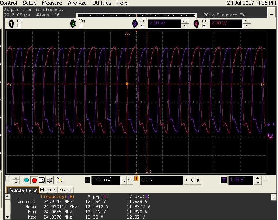
    I tried to replicate customer's setup on THS6012 EVM by replacing the THS6012 device with the THS6002. The THS6002 gain is set to 6V/V (Rf = 1kohms) and the input is 2.1Vpp with 25MHz square wave, similar to the customer's setup. I was able to excite only two channels (driver side) of the THS6002 simultaneously because the THS6012 EVM has only two inputs. As you can see from the below scope capture, the THS6002 outputs do not exhibit the shut-down behavior for 12Vpp output as the customer sees. It does show a slewed output which probably indicates that it would be better to switch to THS3092 for 50MHz frequency.

    Another possibility in-addition to the thermal shutdown, which could cause the THS6002 outputs to not swing properly is when there is maximum output current limit set from the power supply source (switcher/LDO). If the power supply cannot source/sink the amount of current needed for the THS6002 to swing 12V peak, then certainly the output amplitude from the THS6002 will be reduced. Is it possible to know what device is sourcing/sinking current to the THS6002 power supplies?

    Also, not having sufficient supply decoupling at the THS6002 could cause the shut-down issue if the response time of the power supply device (switcher/LDO) is slow. I noticed in the customer's schematic that only one channel of THS6002 has 6.9uF supply cap whereas the other channel has 0.1uF supply cap. Is there a reason for doing it this way? Is the customer seeing the issue only on those channels that have the 0.1uF supply caps?

    Best Regards,

    Rohit


  • Rohit,

    The customer has concluded that the thermal circuitry is most likely causing the issue. He does have a couple further questions:

    The only mistake I made was in assuming I could use all four parts in the package in a challenging multi-channel design (not related to ADSL) requiring 32-channels of high bandwidth amplification in a tight pcb area/space!  Since there is apparently nothing I can do to coax the THS6002 to work for me without a new pcb design anyway, the THS3092/6 is perhaps a better solution, if TI can offer any assurance that it too will not fail in 32-channel collections.  I did a similar design for the same client years ago based on the THS3001 amp which worked well, but DID need liquid cooling!

    My initial checkout of it on the THS3092 evaluation board looks good performance wise on a single channel to provide reasonable 0-12V signal output of 25MHz square wave with +14V/-5V power rails at a gain of 6.  There is an oddity with it however regarding termination and/or loading of my signal generator.  The generator has a “50 ohm output” which is connected via 50-ohm coax to the SMA input of the eval board which is terminated with a 50-ohm resistor.  The input signal looks ok when the op-amp is un-powered although at a lower level than “programmed” on the signal generator.  When the eval board is powered on, the input signal jumps dramatically in amplitude and looks terrible with reflections/overshoot as if very poorly terminated or mismatched!  Granted, the signal generator I am using is not a super high-end piece of test equipment.

    Therefore, before I attempt to put 32-channels of amp on a board with cable terminations at the inputs - - - how can I calculate or at least closely estimate the THS3092/96 part’s non-inverting input impedance when both powered and un-powered (or disabled if THS3096).  I do not want to proceed with yet another time consuming and expensive pcb (and transmission line) design using a part with possible unpredictable behaviors

    Can you comment on his questions regarding the input impedance of the THS3092/96? I know that we cannot estimate the thermal efficiency of the circuit, but is there anyway that we could calculate the total thermal load would be for 32 of these devices on a single board? It seems to me that he is really stretching the design. The thermal performance is normally predicated on the ability of either the copper or an attached heat sink to dissipate the energy, but if the board itself is small this limits the amount of copper etc and thus the ability to dissipate the heat. Let me know if you have any further comments.

    Thanks for your help with this!

    Richard Elmquist

  • Rohit,

    Here are some further comments and questions from the customer:

    With respect to the THS6002 thermal issues, I acquired an IR thermometer and collected some measurements to document whats occurring. 
    On my pcb, with all 32-channels of amps running for a few minutes with the “problem” signal behavior active, the following temperatures were recorded:
    Top surface of a single part – worst one I could find was at a mere 45°C.
    Wider top surface board area over several parts – average temp at 42°C
    Apparently the pcb is doing very well to heat sink and dissipate the power across the pcb.  I have a fan blowing air across the pcb setting on the bench top.
    I also measured the package temperature of the single part that I put in my “breadboard” with no heat sinking.  Again running in free air for a few minutes I was only able to measure a max package temp (top surface) of about 53°C.  I shot it with some freeze spray and the shutdown behavior temporarily diminished slightly but did no go away. The package temp went way down to around -20°C for a short bit.
    Sounds to me like the temp shutdown sensor circuit is seeing some “instantaneous” die temperature due to being located on top of (very close to) an output transistor that doesn’t like the large negative going signal swings.  Or perhaps its just mis-calibrated and not really measuring anything close to the 180°C max temp.  In any case, this behavior makes the part essentially unusable for my application.  I have done everything possible to alleviate any real thermal concerns thru pcb design and heat sinking.  Short of liquid cooling to keep ambient temperature at sub-freezing, I’m giving up and proceeding to a re-design with the THS3096.
    TI should consider revising the THS6002 data sheet to warn anyone attempting to extract full large signal performance from all four amps in the package at the same time!  Or at least reduce the advertised operational temp range of the part to arctic levels <grin> as its certainly not behaving like a typical 0-70°C component should.
    My testing of the THS3092 evaluation board looks good except for the strange loading of my input signal source when its powered.  Unfortunately, I don’t know what my signal generator is really driving it with beyond the fact that it claims to be a “50 ohm output” instrument.  Must not be a super-duper TI high-drive op-amp (kidding).  The only thing I can guess is the 3092, while running with a 2V positive input is experiencing some common-mode saturation or something via the negative input (feedback path) and then exhibiting a very low effective input impedance to the signal generator and creating a badly mismatched signal termination in the process.  Plausible?
    Again, just trying to understand what’s happening before I proceed with another 32-channel attempt!  I intend to use the THS3096 package with power-pad along with the power-down control provided in that part.  Makes it even more important to understand the part’s behavior when its “off”.
    Is the issue he is seeing when he powers the THS3092 something that you have seen before? Can you offer any suggestions?
    Thanks for your help with this!
    Richard Elmquist
  • Rohit,

    I will be out of the office starting Wednesday the 9th. If possible, could your respond before then so that I could send the response to the customer?

    Thanks for your help with this!

    Richard Elmquist

  • Hi Richard,

    In-order to calculate or measure the THS3092/96 part's non-inverting input impedance across frequency when both powered on and off, the best way is to measure the part on a vector network analyzer (VNA). The VNA should provide the input as well as output reflection parameters (S11/S22), which can then be used to estimate the input impedance using the below equation.   

    S11 = (Zin - Zo)/(Zin+Zo)

    where, Zo = 50-ohms and Zin is the required input impedance.

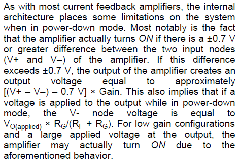
    If the customer sees lot of reflections/overshoot in the input signal, then it is possible to reduce those by using an external low-pass filter (maybe Trilithic) of ~100 MHz BW. The other thing to also note is that if the device input signal goes beyond +/-0.7V or greater when Off, you might actually be turning On the device due to the internal architecture of most current feedback amplifiers. Could this be the reason why he sees difference in input signal levels from the signal generator for higher input swings when powered down?

    Best Regards,

    Rohit

    THS3092 datasheet page 20:

  • Rohit,

    Thanks for your quick response!

    I will let you know if the customer has any further questions.

    Thanks again for your help.

    Richard Elmquist