This thread has been locked.

If you have a related question, please click the "Ask a related question" button in the top right corner. The newly created question will be automatically linked to this question.

HDMI Re-Driver TMDS181RGZR

Other Parts Discussed in Thread: TMDS181, TDP158, SN75DP159

Dear Community,

I just want to clarify, whether can i use HDMI Re-Driver TMDS181RGZR at input side of HDMI2.0 input display port.

As per datasheet, under device application this re-driver is used between Process (TMDS driver) and HDMI output display.


But in my application, i am using this re-driver IC between HDMI 2.0 Input display (TMDS Driver) and FPGA GTH transceiver.

Please suggest me can i go ahead with this Re-Driver.

If this Re-Driver is not applicable to my application, please suggest me other part.

So that i can implement in my design.

Thanks & regards,

Divya

  • e2e.ti.com/.../2129254

    The TMDS181 will work for your application but you might want to read the e2e post above to understand how to connect the TMDS181 to the FPGA.
  • Hi,

    Thank you for the Quick reply.

    Now we are replacing the HDMI re-driver part  to TDP158RSBR.

    Whether this part will support for my application ?

    Thanks & regards,

    Divya

  • Hello Divya,

    We do not recommend using the TDP158 for source side applications. The TMDS181 with the double terminated outputs will better fit your application. 

  • Clarification: TDB158 is intended for source side applications only, not sink side applications. TMDS181 is the better solution for this application.
  • Hi,

    Thanks for the usefull information.

    We are using this TMDS181RGZR in the below applications.

    1)4 lane inputs from Zynq Ultrascale+ GTH bank and outputs to HDMI Connector and

    2)4 lane input from HDMI connector and output to Zynq Ultrascale+ GTH bank

    e2e.ti.com/.../2129254  In this Forum, here it is given the clarification regarding TMDS181RGZR interfaced between HDMI input connector and xillinx FPGA (add 50E pull up resistor to 3.3 near to TMDS181RGZR)

    wether i have to follow the same circuit in my design ? please give the clarification.

    I am waiting for your suggestion.

    Thanks & regards,

    Divya

  • Yes, you will have to follow the same schematic as the other E2E post.
  • Hi,

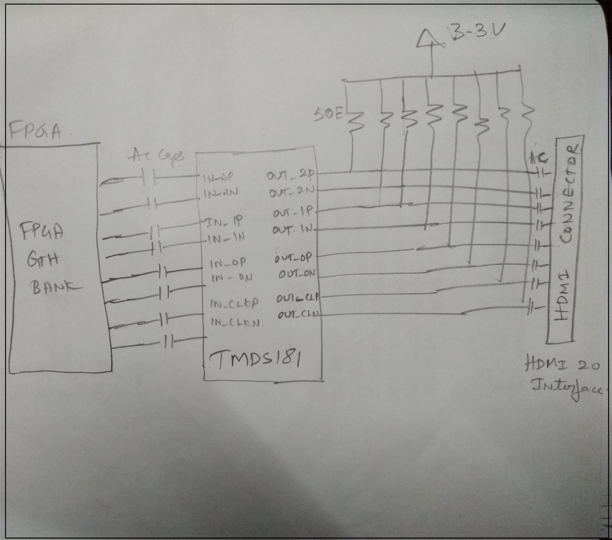
    In the above Block diagram, I have interfaced TMDS181 Retimer between FPGA and HDMI Connector.
    I have connected AC caps between FPGA and TMDS input channels and 50E pull up resistor and AC caps at the output channels to HDMI connector.

    I just wanted to clarify this circuit design is proper or not. if it is wrong please correct it.

    Thanks & regards,

    Divya

  • Hi Divya,

    The TMDS181 device requires standard TMDS inputs, it cannot accept AC-coupled inputs.  The SN75DP159RGZ is a better choice for an application that requires AC-coupled TMDS inputs.  Also why would the TMDS outputs to a standard HDMI connector be AC-coupled?  Is this a custom connector?

    Regards,

    JMMN

  • Hi JMMN,

    Thanks for the information.

    In application of FPGA (source) to HDMI Dispaly (Sink)

    I have planned to use AC Caps at the TMDS181 inputs because it does not satisfy common mode input voltage requirements.

    At FPGA side Common mode output voltage  VCMOUTDC =2.05V, whereas in TMDS181 Common mode input VIC=2.9 (MIN)

    Please suggest how can i proceed ???

    In application of HDMI Display (Source) to FPGA (sink),

    i don't know about the Common mode output voltage at HDMI Display side. At the output of TMDS181 to FPGA i can place AC caps near to FPGA GTH pins (internal biasing enabled) so that we can achive common mode voltage range at FPGA side.

    Above my thought is correct or not ?

     SN75DP159RGZ : Can i use this part for my above 2 applications ??? FPGA (source) to HDMI Dispaly (Sink) and HDMI Display (Source) to FPGA (sink)


    Please suggest me.

    Thanks & regards,

    Divya

  • Divya,

    Please check with the FPGA manufacturer on the requirements for FPGA source to HDMI sink.  If the FPGA requires AC coupling, use the SN75DP159 device.

    The outputs of the TMDS181 or SN75DP159 are standard TMDS outputs.  This means that there must be 50 ohms to 3.3V for current sourcing.

    Regards,

    JMMN

  • Hi JMMN,

    Thanks for the reply.

    Can i interface HDMI display at the input of SN75DP159 and FPGA at the output of SN75DP159. Please provide the reference schematic.

    Thanks & regards,

    Divya

  • Hi Divya,

    Since you have two different applications, you need to use two different redriver/retime devices. The EVM User's Guide for each device has a reference schematic.

    SN75DP159 is designed for AC-coupled TMDS inputs to standard TMDS outputs.
    TMDS181 is designed for standard TMDS inputs to standard TMDS outputs.

    Regards,
    JMMN
  • Hi JMMN,

    Thanks for your support.

    Please clarify below 2 doubts.

    1) Instead of SN75DP159 can we use TDP158 ? beacuse both IC input supports  AC coupled TMDS inputs. 

    2) In case of all 3 (TMDS181, SN75DP159 & TDP1585)  part, at the TMDS output side we have to provide the 50E termination resistors ?

    Thanks & regards,

    Divya

  • Hi JMMN,

    Please clarify on sink & source application. what u mean by sink and source application ?

    1) If we are interfacing Re-driver IC between FPGA (TMDS Source) and HDMI Connector (TMDS SINK) Then where i have to interface DDC singals ?

    DDC_SCL_SRC  & DDC_SDA_SRC to FPGA side ???

    DDC_SCL_SNK  & DDC_SDA_SNK to connector side ???

    2)If we are interfacing Re-driver IC between FPGA (TMDS Sink) and HDMI Connector (TMDS Source), 

    DDC_SCL_SRC  & DDC_SDA_SRC to connector side ???

    DDC_SCL_SNK  & DDC_SDA_SNK to FPGA  side ???

    if it is so, have to provide 5V pull up at connector side DDC lines and 3.3V level pull up FPGA side DDC line or else Voltage level translator is required here?

    Please clarify on above 2 points.

    Is there any issue or errata, or chances of the part obsoletence ?, because our customer wants to support the part for next 20 years.

    I am waiting for your reply.

    Thanks & regards,

    Divya

  • Divya,

    Intended for source side applications:
    SN75DP159 is designed for AC-coupled TMDS inputs to standard TMDS outputs (redriver / retimer)
    TDP158 is designed for AC-coupled TMDS inputs to standard TMDS outputs (redriver)

    Intended for sink side applications:
    TMDS181 is designed for standard TMDS inputs to standard TMDS outputs (redriver /retimer)

    All standard TMDS outputs require termination to 3.3V, these are integrated into standard TMDS sink devices. External terminations are only needed if the TMDS outputs are being routed to an AC-coupled sink.

    We typically recommend customers short the DDC_SRC pins on the redriver / retimers to ground and route the DDC lines by the DDC_SNK pins in "snoop" mode. This is explained in the device datasheets.

    There are no plans to EOL these devices.