This thread has been locked.

If you have a related question, please click the "Ask a related question" button in the top right corner. The newly created question will be automatically linked to this question.

High gain transimpedance amplifier

Other Parts Discussed in Thread: ADC161S626, LMP7721, OPA277, ADS1251, OPA847

Hi everyone,

I am a physicics trying to design a photodiode amplifier, I have experience in electrical design, but this one is a real challenge for me.

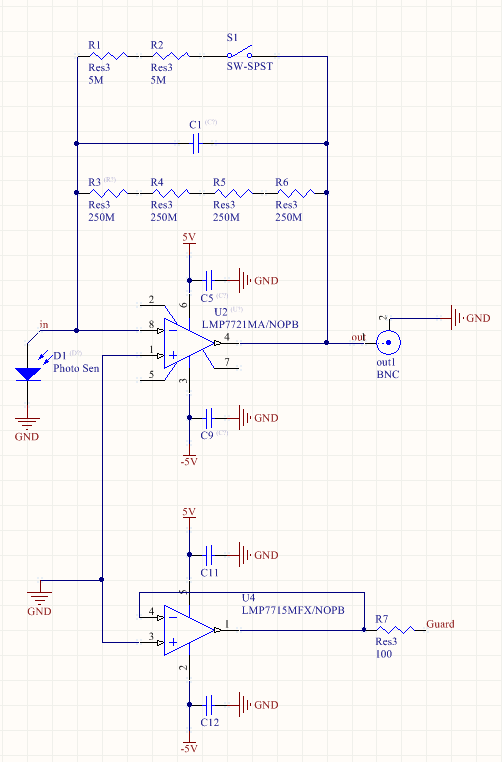
I am designing a photodiode amplifier to measure very low light level at a frequency around 15kHz. My photodiode capacitance is 140pF. The minimum current that I need to detect is around 0.3pA and the maximum is 0.3uA.  The scale is very broad so I think I will need different amplification level. This is the first thing that I am not sure about.

1) How to implement different transimpedance amplification level? I though of using ADC161S626 as an interface and a DAC would provide different Vref for the ADC converter. Is this the best way to proceed?

2) The second thing that I have a problem with is the 0.3pA at 15kHz. There is so many choices of op amp that I have become lost. I think the best way to procceed would be to define the maximum amplification I can get at 15kHz considering stray capacitance and then choose an ADC with sufficient bits to get the accuracy I need to get to 0.3pA.

So far, I have looked at the LMP7721, OPA277 and OPA847 with TINA (and a simple photovoltaic circuit) and the maximum I got (while having 15kHz) was a gain of G=5M with a capacitance Cd=1pF. That gives me a minimum of 1.5uV to detect with the ADS1251  (19bits, 20kHz, Vref=0.5V). Is this realistic??

3) Would a phase compensation circuit be usefull in this case?  http://www.eetimes.com/electronics-news/4164311/Current-feedback-op-amps-save-power-in-fast-photodiode-applications

Thanks for your help

  • What is the value of Rin for the  LMP7721?

  • Hi Paul,

    I'm not phisicist, I'm engineer, and whatever I answer here is not based on calculations, they're here just my "feelings".

    Before you do anything, please don't forget to read Paul Grohe's articles:

    http://www.edn.com/design/analog/4368681/Design-femtoampere-circuits-with-low-leakage-part-one

    http://www.edn.com/design/analog/4375459/Design-femtoampere-circuits-with-low-leakage---Part-2--Component-selection

    http://www.edn.com/design/analog/4395651/Design-femtoampere-circuits-with-low-leakage---Part-3--Low-current-design-techniques

    A further reading is from Bob Pease: What's all this femtoampere stuff, anyhow? Google will find it.

     It is possible to change the transimpedance by changing the feedback resistor. But, since you will play in the sub-picoampere range, the switching element can be critical. I don't think that any semiconductor switches can give you the required performance due to their charge injection and leakage. Reed relays are somewhat better, but in the sub-pA world, the fewer the components you build in, the easier your life will be.

    I wouldn't choose a SAR type ADC to digitize the signal. At such a low level, integrating type ADC's provide the best signal to noise ratio. If a dual slope converter is too slow, try a sigma-delta architecture, like ADS1251 or something similar.

    Also, due to signal to noise ratio and due to accuracy, I wouldn't make the reference voltage variable. Maybe, I'm too conservative, but reference is reference. It should come from a dedicated voltage reference IC, must be stable and very well decoupled. A DAC introduces noise and inaccuracy. When you lower the reference voltage of an ADC, you also reduce the signal to noise ratio, the result can be that lower bits representing a true random number instead of your signal.

    Isn't it possible to make the input light somewhat stronger? Some optical lenses, for example? Is it possible to keep the electronic in a cold chamber?

    Don't thrust in any simulation software, always build a proto. Would you lead the input signal on an FR4 board? Than read the above articles once more.

  • Thanks Bela,

    nice reading, this will help me a lot when I design the PCB itself. I need a good schematic now.

    1) Regarding the multi-level gain, I also though that a switching element would add too much leakage to be usable. However, I found this circuit allowing different gain to be used. http://www.diy-electronic-projects.com/p212-Picoammeter-circuit-with-4-ranges What do you think?

    2) For the ADC I take good note of what you say. For the signal to noise ratio I found out that with a Gain=1G, I could have a SNR=10 at 100Hz with 0.3pA. The AC transfer is -3db at 100Hz using a 1pF parallel capacitor. On the other hand, a Gain=10M would give me a SNR=10 at 7Hz only even if the AC transfer would allow a signal to get up to -3db at 2kHz.

    This means that having different gain would help me have good SNR in the pA range at ~100Hz AND good SNR in the nA range at frequencies much higher. It also means that having a high resolution ADC won't be of any help for bandwidth improvements. I would have better SNR and bandwidth using different gain or is it me thinking wrong?

    The input light, there is no way to make it stronger. We already use high quality optical components. However, we will need to be flexible on the frequency. I will try to increase the bandwidth as much as I can, but without compromising resolution.

    Best Regards

  • I check the multi-level gain circuit I sent in the previous message and this is not good for transimpedance circuits.

    Here is the circuit I am thinking of using.

    Would the mechanical switch add too much noise? Or would another kind of switch be better?

    If I put a BNC at the ouput in parallel to the ADC, would I add a lot of noise? I am thinking of using a DAC after the ADC for the BNC output.. what do you think?

  • Dear Paul,

    let me recommend one more reading:

    Jerald Graeme: Photodiode Amplifiers

    http://www.amazon.com/Photodiode-Amplifiers-OP-AMP-Solutions/dp/007024247X/ref=sr_1_1?ie=UTF8&qid=1356037571&sr=8-1&keywords=jerald+graeme

    The behaviour, analysis, construction and AC performance is very well detailed there. And it's not hard to read too.

    I do not like that schematic from diy-electronic-projects.com. It is not a transimpedance amplifier, it is a voltage amplifier, whatever the literature says. It will successfully amplify it's own offset. I suppose, it is a waste of time to try it (because I tried and I wasted some time on it :-) )

    The second schematic may work. I think you need 10GOhm in the more sensitive range, to reach 3mV at 0,3pA and 3V at 300pA. The lest sensitive range looks correct. This scaling is realistic, but don't forget about noise. You may not expect a clean signal when at the 300fA niveau.

    The reed relay doesn't inject noise, except when it switches. But it may inject leakage current. There are electrostatically shielded versions, I would try these. Choose a reed relay, which has an insulation resistance specified at 1012 Ohm. Just for safety, I would put the relay on the other side of R2. That's a lower impedance point. This way the track from R2 to the input of the opamp can be shorter, and may be in the air wired. When you wire the reed relay, the GND end of the coil must be closer to the glass tube in the reed relay, and it is better to connect it to the resistor side. The other side can be switched between GND and Vcc to switch the relay, This way you induce smaller error signal into the opamp through R2 when the relay switches. How to find out, which end of the coil wire is closer to the glass? Good question, I'd break one relay.

    I don' understand correctly, what would you like with a BNC connector, but if you put one on the output of the LMP7721, I don't expect any noise injection there. In case it goes to the outside world, I would recommend a unity gain buffer, just to isolate somehow the outer world from the LMP7721. There are chopper-stabilized opamps with very low offset and drift, they aren't expensive, just drop in one.Nobody knows, what will be once into this connector plugged, and where goes that cable.

    Please note that high resolution ADCs often require differential input signal. A GND based single ended signal may not work properly there, so you need a single ended to differential converter, formed of two opamps and some accurate resistors, or formed of an instrumentation amplifier.

  • Thanks Bela,

    for the DIY schematic, it was in fact a waste of time, sorry about that!

    About the 10GOhm amplification, I take good note of what you say. I will try and see what to expect with regards to SNR and bandwidth.

    Thanks for the input on how to solder the reed relay, I wouldn't have though about it.

    To clarify things on the output, I want to have a digital ouput, so I need an ADC. This way I think I may have more precision (when transferring the results to a uC)  than with a direct analog output connected directly to a BNC cable. However, I also need a BNC even if I loose a little precision (due to SNR) on that output, to give me the choice of using digital data or analog signal. For the BNC connector, you are right, a simple buffer would isolate it from the rest of the schematic, good idea.

    I have 2 questions remaining:

    1) I search for through hole resistor (10MOhm+) so I could solder them above a board in series to decrease their capacitance, but the only one I found where like 1 inch long(!!!)http://www.digikey.com/product-detail/en/SM104035006FE/SM104FE-500M-ND/824210 while the surface mount are 0805 type. Is there a kind of resistor that I missed that are shorter?

    2) I used the low impedance node to drive the guard ring. I see that this is usually the Vref of the output. However, can I use the GND as the Vref of the guard ring or do I loose any effect when doing that? I also though to use a negative Vref (to have more range), but that would make the GND of the BNC connector negative which I don't think is good.

    P.S. I bought the book, it seems nice.

  • Hi Paul,

    first of all: LMP7721 has a max supply voltage at 6V specified. it means max 6V between pin3 and pin6. It does not mean max. +/-6V!
    Please ground pin 2, 5 and 7 as well. Pin 2 and 7 must be connected to the guard potential.

    Maybe Digikey doesn't have a stock of such a high ohmic resistor? Well, here are a few resistor manufacturers:

    SRT-Resisitor Technology
    RCD Components
    Micro Ohm Corporation
    Willow Technologies (I think they're distributors)
    Welwyn -TT
    Ohmcraft

    You may also look at Mouser, Avnet, or other distributors.

    10Gohms are not so extreme values, even Vishay produces it. It is also feasible that you connect a few smaller resistors in series. If you can keep your PCB clean, they may lay on the board.

    In your case the guard ring will be at GND potential, until you insert a resisrot between pin1 of U2 and GND. (I wouldn't do that).

    I'm going home to christmas, I will be unable to answer quickly.

    Therefore, it is not necessary to buffer this potential. The buffer amplifier (U4 on your schema) only introduses offset, a bit of noise, extra power consumption and extra component costs. Nothing else. When you lay your circuit out, employ a solid GND plane due to its low impedance and shielding capability. The guard ring must almost be isolated from this GND plane, except that it is connected to it by one and only one point. This way you can ensure, that no current flows through the guarding. In other words: you have to construct the guard ring so, that it is on GND potential but current doesn't flow through this guard ring. Even a few microamps.

  • Thanks a lot! Have a good holiday!

    I will have the voltage changed to ±2.5V and remove the buffer amplifier!

  • I have another question! I found that reed relays can be sold with 50ohm coaxial shield. Is this something that could improve the noise resistance of the switch if connected to the guard shield?

    http://www.cotorelay.com/index.php?option=com_content&view=article&catid=34%3Areed-relays&id=124%3A9900-reed-relay&Itemid=54

  • This Coto 9900 type relay seems to be a good choice. The 50 Ohm impedance plays a role in high frequencies. This reed are able to switch in the GHz range, so impedance there is important.

    Since your transimpedance in the higher range is only 1MOhm, I don´t think, you will have too much of a problem. Even the 10GOhm range is not extreme, it is feasible. I do talk about DC precision and noise, not about AC bandwidth. You have to build a proto and test it for bandwidth yourself.

    Good luck! (I hope you don't build something for weapons :-) )

  • lol no weapons no! 

    I will be doing to proto very soon (after the holidays).

  • The high value resistor have a capacitance around 1pF.  http://www.ohmite.com/cat/res_minimox.pdf

    Can I remove the 1pF capacitor in my schematic since it is already "generated" by the resistor?

  • Hi Paul,

    this question cannot be answered through the internet. Build your first proto, and if it oscillates (which is, according to Mr Murphy, the normal behaviour of any newly built amplifier), than you can start to compensate it:

    http://www.ti.com/analog/docs/litabsmultiplefilelist.tsp?literatureNumber=sboa055a&docCategoryId=1&familyId=1481

    Although there are a lot of literature, how to compensate the transimpedance amplifier, they all lack of one thing: you cannot be sure, how much the photodiode's capacitance is, and how much is the amplifier's input capacitance is. There's something in the datasheet, but it varies with temperature, with bias voltage, varies piece-to-piece, manufacturer-to-manufacturer, so I say, drop in some capacitance parallel to the feedback resistor, test it again, try another diode, and do this until it works good, or you reach the deadline or until the working hours are all over :-) too much of feedback capacitance gives stability but reduces bandwidth.

    When you think it's already stable, build a small series and test them piece to piece thoroughly.

  • With reference to the post by Bela giving a reference to the app note:

    http://www.ti.com/analog/docs/litabsmultiplefilelist.tsp?literatureNumber=sboa055a&docCategoryId=1&familyId=1481

    you may also find the following app notes useful: sboa060, sboa061 and sboa035. As the compensation feedback capacitor is often small and not well known it is possible to produce a variable value by resistively potting down the output signal and using a larger more available capacitor fed back from the potentiometer junction. This causes the effective capacity to be lowered by the potentiometer attenuation. This can then allow ready adjustment to give good and stable response. Since the required feedback capacitor is determined by the input capacity of the system (for stability against oscillation) then increasing the feedback resistor to achieve increased signal gain necessarily results in decreased bandwidth.

    Scott Hamilton.

  • Hi,

    I haven't had time to finish the circuit, but It is almost complete now. I am in the process of finishing the PCB routing. However, I have another question bugging me.

    I made a guard ring and connected it at only one point using a 0ohm resistor to reduce current going through the guard ring. However, what do I do with the photodiode D1. It is connected on the high impedance node on one side and connected to ground on the other side. I looked http://www.edn.com/design/analog/4395651/2/Design-femtoampere-circuits-with-low-leakage---Part-3--Low-current-design-techniques and it seems that the other side is connected to the guard ring. My problem is that there will be some current going through that. So the question is, should I connect to ground or through guard ring? or maybe use this pin as the connection between GND and Guard?