This thread has been locked.

If you have a related question, please click the "Ask a related question" button in the top right corner. The newly created question will be automatically linked to this question.

AFE031 SPI Trouble

Other Parts Discussed in Thread: AFE031, TMS320F28027, CONTROLSUITE

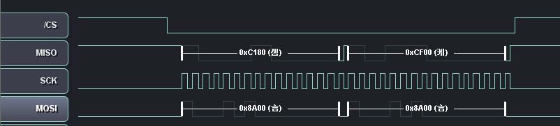
  I am trying to interface the AFE031 via SPI to control the DAC. The output is changing as I write to SPI but not as I expect. I suspect that the SPI mode is incorrect, is there a way to tell the AFE031 which mode to expect? I have read the data from a logic analyzer and am quite certain that my SPI signal is sending the proper data. Any other info regarding the AFE031 would be very much appreciated as  I find the datasheet and Analog Front End Design Note to be very brief.


 I have attached my code and would appreciate if you could take a look at it. It is very simple

http://pastebin.com/pjkMQaN4

  • Hello dmh43,

    I will be more than happy to assist you.

    Please make sure you are using the following sequence to write to the DAC:

    • Set CS low.

    • Set the DAC pin (pin 7) high.

    • Write a 10-bit word to DIN. The DAC register is left-justified and truncates more than 10 bits.

    • Updates the DAC output by driving CS high.

    The output of the DAC can be observed on pin 14 after it has gone through the Tx_PGA. Such output is given by the following equation:

    Please note that the codeword passed onto the DAC is a 10 bit codeword.

    The way to tell the AFE031 which mode to expect is by driving the DAC pin (pin 7) high.

    Hope this helps and please do not hesitate to contact me if I can be of further assistance.

    Best regards,

    Jose

  •  Thanks for your response Jose. It seems that my problem is that I am not communicating properly with the device. I am trying to read the die ID but every time I get a different result. This suggests that I am doing something wrong with the SPI communication. There are timing diagrams for both SPI mode 3 and SPI mode 0. How do I tell the device which to expect?

     When I write 183 to SPI in DAC mode, the output on pin 14 is 1.65V. The signal also looks very noisy (15mV pp).1.65V is also the constant in the equation that you gave me so I think that suggests that I was able to enable the DAC via SPI. Any ideas?

  • When cycle the power, the output of the DAC goes back to floating. When I run the code again, the output is sometimes 0V, sometimes 1.65V and sometimes 700mV. I think this strongly suggests something is wrong with the communication. When I send 0x8A00 to read the device ID, I get a different result every time.

  • Is there any documentation for this chip other than the datasheet and the front end design note? Where did you get that equation for the output of the DAC? I dont think its in the datasheet

  • Hello dmh43,

    Aside from the datasheet and design note there is no other documentation for the AFE031.

    The equation comes from page 3 of the datasheet where the specifications of the transmitter and DAC are given. Please see image below.


    After a power cycle (and after a soft reset)  the DAC plus all internal references in the AFE031 will be disabled. In order to see meaningful DAC outputs you need to enable at a minimum:

    1)    the TX block (by setting bit 1 of register 0x01),

    2)    the DAC (by setting bit 5 of register 0x01),

    3)    the REF2 block (by setting bit 2 of register 0x03).

    With regard to reading the device ID, please make sure you perform two consecutive read cycles onto register 0x0A since the AFE031 presents the previous transaction R/W bit and address for the first 8 bits on SDO followed by the AFE031 contents that correspond to the address field in the previous read cycle. A single read cycle will not shift out the contents of any register.


    Indeed, you could have something wrong with your communication to the SPI interface. Feel free to append logic analyzer or oscilloscope captures onto the body of your post; I can review them to see if there is any timing issue in your commands. Please include and clearly label the signals from pins 3, 4, 5, 6 and 7.

    Hope this helps and please do not hesitate to contact me if I can be of further assistance.

    Best regards,

    Jose

  •  Thanks for the help Jose, I'm still having some trouble though. When I read the die ID I get 0x8000, the revision gives my 0xCF00 I am not sure if that is correct. 

     I am using the TMS320F28027. This is a screenshot from a logic analyzer shoing the transmitted and received data after the first SPI_write command is issued 

    Here is my code again: http://pastebin.com/9kt6a45A

    Any Ideas what the problem might be? Any advice on what to check or look for would be much appreciated as well. Thank you


  • Sorry, forgot to Label the pins in the Logic Analyzer snippet. CS is pin 6, MISO is pin 5, SCK is pin 3, MOSI is pin 4.

  • I was able to get a reasonable output from the DAC 

     I figured out that the DAC pin was not high when I thought I was writing to the DAC register. I inserted some manual delay to ensure that the pin would be high during the time I was writing to the DAC register; is there any better way to do this?

     Also, I seem to be unable to generate any output outside the range from 700mV to 1.4 V. Any idea as to why this might be happening? I am making sure to left shift the bits 6 times before I write to SPI_tx since the DAC is left justified 10bits

  • Hello dmh43,

    One problem I see in the image of the SPI transaction you attached is that it is a single 32-bit transaction. When reading or writing into the control and data registers of the AFE031 you must toggle the SCLK line 16 times, shifting 16 bits into the AFE031 MOSI pin (DIN, pin 4) and shifting out 16 bits from the AFE031 MISO pin (DOUT, pin 5). After such transaction is performed you must raise the CS line and then lower it again before you start the next transaction.

    I’ll be more than happy to review further logic analyzer screenshots from your application once the CS toggling frequency has been fixed. Incorrect timing on the CS line will yield incorrect results on the DAC output and register read/write operations; I suspect that is why you are unable to generate any output other than 700mV and 1.4 V.

    Best regards,

    Jose

  • http://pastebin.com/0AYZgRgb

    The problem I am having is that I dont know when all the SPI data has been transmitted so I dont know when to set the DAC pin high to write to the DAC registers. How can I determine when all SPI transfers have been completed?


  •  I still have not figured out why the DAC is behaving oddly. When I write 0 to the DAC, it gives me 222mV, when I write 1<<6 the DAC outputs 425mV, 512<<6 gives me 324mV and 0xFFFF gives me 222mV. Any ideas what this could be?

  • Also, as for what you mentioned about 32 bit transfers, I have made sure to raise CS between word transfers. Also, I am using the C2000 controlSuite library and here is my code once again:

    http://pastebin.com/yuTub3zm


  • Hello dmh43,

    As the designer of your system and programmer of your code, you get to decide when to set the DAC pin high and when to set it low; once again, please make sure you adhere to the sequence I indicated on Jun 11 2013 10:52 AM.

    I do not know why when you write 0 to the DAC it gives you 222mV; I suspect you are not writing 0 but you are writing something else.

    I will be more than happy to help you troubleshoot your system and the most effective way to do that is to observe the signals present in the SPI interface and the output of the TX_PGA. Please acquire and paste in the body of your next post (just as you did on Jun 14 2013 01:29 AM) the logic analyzer signals present in pins 3, 4, 5, 6 and 7. Please make sure you label them clearly.

    In addition, I would be interested in observing oscilloscope (not logic analyzer) captures of pins 3, 4, 6, and 14 so that I can see the analog level at the output of the TX_PGA.

    Reviewing your code will be useless unless we have a reference on what signals you are applying to the AFE031 and what signals are coming out of it.

    Best regards,

    Jose

  • Thanks for your patience Jose. Here is my code for reference with the screenshots http://pastebin.com/PZ9V9w7C

    Here are some logic analyzer screenshots. As before, CS is pin 6, MISO is pin 5, MOSI is pin 4 SCK is pin 3 and DAC is pin 7. Also, all the scope screenshots are of pin 14

    First I write 0x8B00 to read the DieRev

    I write 0x8B00 a second time to push the values through the SPI shift registers and get the actual value I am looking for which should be 0x9F00 but it is different every time I run my code. Also, the value that I get in my TMS320 when I run SPI_read() at this point is 0x1F00.

    I write 0 to the DAC registers. Here is the output: 

    I write 0x0001<<6 (which evaluates to 0x0040) to the DAC registers, this is the output: 

    And the logic analyzer: 

    Also here is what I get when I write 512<<6 (0x8000): 

    Thanks again for your help

  • Changing the SPI mode to have a phase shift gives me consistent results when reading the DieRev (i get 0x0B00) 

    I have noticed something. In the code I posted above, I set the DAC pin high right after I send an SPI signal to enable REF2; I dont think that I gave sufficient time for the signal to be received. When I insert a delay after writing the SPI signal, REF2 is enabled (which I can tell from pin 14 going to 1.65V) but no matter what I write to the DAC register, the output stays at 1.65V.

  •  I am able to get the output I expect from the DAC. The changes I made was only to move around some of the SPI commands. Instead of enabling the references then enabling the DAC, I enabled the DAC first.

     I am having trouble communicating with the device at higher speeds; the TMS320 SPI module works in such a way that the CS signal stays active between consecutive writes to the SPI channel. The AFE031 requires a rising edge on CS. How can I get this to work?

  • Hello dmh43,

    I am happy to see that you can obtain the expected DAC outputs.

    Indeed, as you can see in page 12 of the AFE031 datasheet, it is necessary to raise the CS line for SPI transactions to be processed. For more information on how to program the specific C2000 microcontroller you are using I suggest consulting its documentation at http://www.ti.com/lsds/ti/microcontroller/32-bit_c2000/overview.page

    Another good resource is the C2000 forum at:

    http://e2e.ti.com/support/microcontrollers/c2000/f/171.aspx

    Best regards,

    Jose

  • Hello Jose,

    I have a question to consult you : I can read the values of Regsters in AFE031,but I can't program them as I expect,that is ,I can't write them,why?

  • Hello Juan Wang1,

    Probably the issue is the most significant bit of your SPI transaction. Remember that a leading 1 means read and a leading 0 means write. Perhaps you are not swapping that bit from 1 to 0 when you perform a write operation.

    Hope this helps.

    Best regards,

    Jose

  • Hello Jose,

    Thank you for your answer first. I think have  set the leading 0  when I perform a  write operation,but I still can't write ,the read value is also the default.Could you help me ?

    Best regards,

    Juan Wang1

  • And the read value of RESET Register is 0XC0 or 0X40, is the chip of AFE031 bad?

    Looking forword to your reply  as soon as possible. Thank you !

  • Hello Juan Wang1,

    I do not know why you are experiencing problems. Please include oscilloscope captures of the signals present in the following pins: SCLK, DIN, DOUT, CS.

    The captures should be taken as close as possible to the AFE031 and please label them clearly.

    Also, please make sure the SD pin is held low during the SPI operations.

    Best regards,

    Jose

  • Hello Jose,

    Thank you for your answers first.

    I have read the value of AFE031 Registers,but the value of RESET Register is 0x40,which means I_FLAG is 1.I think this is a error but I dong't know why.

    And ,when I set the DAC PIN a 1 and send data to DIN(I can see the wave from DIN pin with a oscilloscope),I can't see the wave from PA_IN and PA_OUT.

    Looking forword to your reply  as soon as possible. Thank you !

  • Hello Juan Wang1,

    The value you read in the RESET register is not an error. Internally, the conditions that cause the IFLAG to be set when an over-current event happens are the same conditions present when the PA is disabled. The RESET register will real 0x40 as long as the PA is disabled or has been disabled before reading such register. In order to properly interpret the IFLAG bit, one must enable the PA and then reset the bit.

    I cannot help you troubleshoot your DAC write iperations unless you show me the signals you are transmitting onto the SPI bus. I will be happy to review the signals present in the SPI interface and the DAC pin; please include clearly labeled oscilloscope captures.

    Best regards,

    Jose

  • Hello Jose,

    I don't know what do you mean.Is the sequence of writing the registers of AFE031 wrong?The sequence I have used is as follows:

    And the read values are:

    coresponding to the  registers:

    ENABLE1,GAIN SELECT,ENABLE2,CONTROL1,CONTROL2,RESET,DIE_ID,REVISION

    Looking forword to your reply  as soon as possible. Thank you !


  • Hello Juan Wang1,

    I assume that the first field in your “write” command is the register address, and that the second field is the information to be written.

    If that is the case, you are attempting to perform the following actions:

    1)      Resetting the AFE031 (this will set the I_FLAG and such flag will remain enabled until the PA is enabled and the I_FLAG bit is reset.)

    2)      The following blocks are enabled: PA, Tx, Rx, DAC. The following blocks are disabled: ERX, ETX.

    3)      The logical OR combination of an over-temperature event or over-current event will trigger the  open-drain active-low INT pin. The INT pin will be activated now because you have not cleared the the PA output stage has not been enabled yet.

    4)      Tx filter and Rx filter are set to CENELEC B, C, D bands.

    5)      The PA output stage is enabled. The  voltage references (REF1 and REF2) and zero crossing detectors are disabled. Note that you will not be able to observe any meaningful signal coming out of the signal chain until you enable the voltage references.

    6)      RXPGA1 is set to a gain of 1 V/V,  RXPGA2 is set to a gain of 16 V/V, TXPGA1 is set to a gain of 1 V/V.

    You must enable the voltage references before sending any data to the DAC.

    Best regards,

    Jose

  • Hello Jose,

    You are right ,the  first field in my “write” command is the register address, and that the second field is the information to be written.

    I have revise the information of AFE031  registers according to your suggest.

    And the value of "read" are:

    And the I_FLAG is still 1.Any ideas ?

    Looking forword to your reply  as soon as possible. Thank you !

  •  And the wave of the PIN 3,4,6,7 are the following:


    "2"is "DAC","4"is "CS",


    "2" is "DAC";"4" is "SCK";"1" is "DIN",  write the number of "0xF0" and "0x00";


    "2"is "PA_IN";"4"is "SCK";"1"is "DIN",the send number are cycle of "0xF0" and "0x00";
    This is the larger version of the former waves.
    Because of the limited experimental conditions,  there are only there probes.
    Could you give me any suggestions? And why the wave of PA_IN is as the probe of "2"? Thank you for your patience.
    Looking forword to your reply  as soon as possible.
    Have a good weekend!
  • Hello Juan Wang1,

    There is a problem with your use of the DAC pin. You are toggling the DAC pin at the same time you toggle the CS pin and that will cause problems. During DAC sample transmissions you must keep the DAC pin high.

    Also, you are not toggling the SCLK pin enough times, remember that DAC samples consist of 10 bits. Please refer to page 28 of the AFE031 datasheet for a complete description of the DAC block. You muust provide at least 10 click cycles on the SCLK pin when the devices is set in DAC mode; currently you are only toggling the SCLK pin 8 times and that is insufficient.

    Hope this helps.

    Best regards,

    Jose

  • Hello Jose,

    I'm sorry to bothor you .Thank you for your answers.
    I  have receive the ideal  DAC result  at PIN 14.But I don't understand the wave of PA_OUT.And how  the PA  amplify the signal ? Only with the gain of 6.5V/V? Are there any other formulas for the PA?

    Looking forword to your reply  as soon as possible.


  • Hello Jose,

    I have a new question about the frenquency of SPI in AFE031.

    I have set the 031 DAC mode.And set the SCLK in SPI 20MHz..I want to sent 12  points (sent a 16 bits binary represent a point) to simulate a 150KHz sine wave,but  the frenquency can't up to 50KHz, and the extreme frenquency is 20MHz/16 bits/12 points=104KHz..Is the frenquency of 150KHz beyond the range of FAE031?

    Or the derivation above has some wrong?

    Thank you !

  • Hello Juan Wang1,

    Your derivation is correct.

    If you want to synthesize 150 kHz signals you will need to pass 10-bit binary data into the AFE031 DAC.

    Best,

    Jose

  • Hello Jose,

    Thank you for your answers,but I also have some questions .

    How can I only pass 10-bit binary data into the AFE031 DAC? If I pass 8-bit binary (1110,1011) , the valid data in the DAC register is 00,1110,1011 or  1110,1011,00,or something else? Can I only send 8-bit binary data into the AFE031 DAC?

    Thanks!

  • Hello,it's me Gokhan. I am interested in AFE031 in order to finish my thesis which is designing a PLC Modem.

    I have read earlier post about programming AFE031. I am going to use Stellaris  on my modem.

     Is there any example code for communication between Stellaris and AFE031 through SPI ?

    I just need to read and write  to  AFE031. 

    thanks.

  • Hello Gokhan Satilmis,

    We do not have example code for Stellaris. The TI PLC firmware is specifically created for C2000 microcontrollers.

    The software for PLC is available through controlSUITE (www.ti.com/tool/controlsuite). The software allows a host controller (potentially your Stellaris) to establish UART communication with the C2000 in charge of the modem’s hardware abstraction layer, physical layer, and media access control (mac ) layer. The host controller would communicate with the C2000 through a convergence application programing interface.

    The C2000 forums are your best resource for more specific questions on TI’s PLC software.

    Hope this helps and best regards,

    Jose

  • Hi Jose,

    I have a question regarding AFE031 SPI communication.

    Currently I'm using F28069 micro and using SPIA to communicate with AFE031. The setup is 16bit transfer, 750kHz clock.

    My SPI routine was based on the hal_spi.c file that came in hal_afe project, in PRIME_V8010_DDK_package.

    I've scoped the SPI signals and they look good but I was having a problem where, when I read a register, I was not getting the correct value back.

    After some investigation I have fixed it but it does not quite match up with what's shown on the AFE031 datasheet.

    In Figure 4 of the datasheet shows the Read operation for the SPI mode. It illustrates to me that you should send 16bit value which consists of the address and read flag bit first. Next you should send some value to receive the data at the address. My routine for this goes something like this:

    Uint16 hal_spi_read(Uint16 a)
    {
    AFE031_CS = 0;
    
    SpiaRegs.SPITXBUF = a;
    
    while(!SpiaRegs.SPIFFRX.bit.RXFFST);
    
    val = SpiaRegs.SPIRXBUF; // dummy read
    
    SpiaRegs.SPITXBUF = a; // dummy write to receive the data
    
    while(!SpiaRegs.SPIFFRX.bit.RXFFST);
    
    val = SpiaRegs.SPIRXBUF;
    
    AFE031_CS = 1;
    
    return val;
    
    }

    However, with this routine I was never receiving the correct data. What I found was that the first read of SPIRXBUF (dummy read) actually contains the expected receive data. 

    Now for this to match up with what's indicated on the datasheet, maybe we are supposed to use 8bit SPI communication, rather than 16bit? 

    It will be great to see a better illustration of the expected SPI communication in the AFE031 datasheet.

    Could you help me out with what I'm seeing here and confirm if AFE031 is expecting 8bit or 16bit SPI communication? Note that I'm not using DAC mode at the moment, it's purely reading/writing registers on AFE031.

    Thanks,

    Ayaka

  • Hi Jose again,

    Actually, I spoke a little too soon.
    After looking at the datasheet, I didn't realise there was supposed to be a toggle in chip select when you do a read.
    I've modified the read function to below and it's working as expected!

    Uint16 hal_spi_read(Uint16 a)
    {
    AFE031_CS = 0;

    SpiaRegs.SPITXBUF = a;

    while(!SpiaRegs.SPIFFRX.bit.RXFFST);

    val = SpiaRegs.SPIRXBUF; // dummy read
    AFE031_CS = 1;

    DELAY_US(10);

    AFE031_CS=0;
    SpiaRegs.SPITXBUF = a; // dummy write to receive the data

    while(!SpiaRegs.SPIFFRX.bit.RXFFST);

    val = SpiaRegs.SPIRXBUF;

    AFE031_CS = 1;

    return val;

    }
  • Hello Ayaka,

    I am glad that your routine is working now. Let me know if I can be of any further assistance.

    Best regards,

    Jose
  • Hello everyone

    I have the same doubt that Juan wang had about the SPI, does anyone know the answer to this question?

    juan wang1 wrote the following post at Jul 24, 2014 6:45 AM:

    Hello Jose,

    Thank you for your answers,but I also have some questions .

    How can I only pass 10-bit binary data into the AFE031 DAC? If I pass 8-bit binary (1110,1011) , the valid data in the DAC register is 00,1110,1011 or  1110,1011,00,or something else? Can I only send 8-bit binary data into the AFE031 DAC?

    Thanks!

  • Hello Elvys Collado,

    Passing 8-bit words into the AFE031 DAC will result in unpredictable DAC outputs. The correct approach to obtain the desired DAC output is to feed a 10-bit word to it.

    Best regards,

    Jose

  • Thank you Jose


    Since most of the common uC use 8 -16 bits words, how you solve this problem? Sending 16bits and  letting the chip truncate the data? or you know any other way?


    Best regards,


    EC

  • Hello Elvys Collado,

    Sending 16-bit words will accomplish the task.

    Best regards,

    Jose