This thread has been locked.

If you have a related question, please click the "Ask a related question" button in the top right corner. The newly created question will be automatically linked to this question.

the circuit of pulse generation using TLV3501 and OPA357

Other Parts Discussed in Thread: OPA357, TLV3501, REF5025, TPS54550, TL3016, LM5113

Hi all,

Samsung inquired for the circuit of pulse generation using  TLV3501 and OPA357.

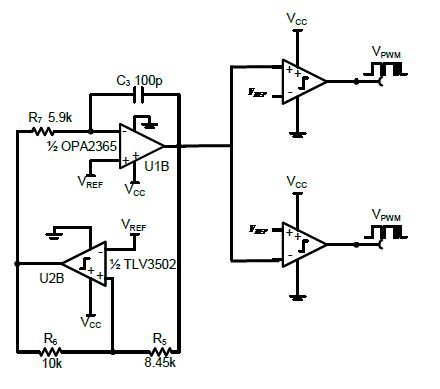
The circuit is as below.

 They did simulation using Tina file for triangle wave generator that you gave me at E2E before. However, they could find that the triangle wave is changed depending on the value of resistors. Even if the value of resistors was changed a little bit, the triangle wave was changed much.

 So the question is how much tolerance of resistors has an inpact on the period(or frequency) of total PWM pulses when the PWM pulses are generated through comparators after triangle wave occur.

That is, they would like to know the range of error due to the resistor.

The reason why they asked this question is that there is +/- allowable tolerance frequency at specific frequency range.

Also, when the capacitances are added at Vref, how much the capacitances have an influence on output voltage. (that is, parallel capacitor at Vref for both of TLV3501 and OPA357)

Would you give me the answers as soon as possible?

Thank you.

Warm regards,

Sammy Jeon.

  • Sammy,

    This oscillator circuit is not meant to be extremely accurate in terms of frequency. From my TI Precision Design (http://www.ti.com/lit/ug/slau508/slau508.pdf), where part of your schematic came from, The frequency of oscillation is:

    Every component in the circuit has an effect on the oscillation frequency. Even using 1% resistors and 5% capacitors I would expect up to a +/- 10% tolerance in the triangle wave frequency. 

    As I describe in the TI design, the proper process for designing this oscillator is to chose the values of R5 and R6 first with this equation:

    Where V1 is the comparator output above or below the reference voltage. Because I used a 2.5V reference voltage, and the comparator output could reach 5V, V1 in my circuit was 2.5. R5 and R6 determine the amplitude of the output triangle wave and must be chosen so that the op amp does not saturate at the power supply rails. Therefore R5 must be less than R6

    Once you have selected R5 and R6 you can now calculate the values of R7 and C3 which will give your desired frequency. 

  • 4377.TLV3501 & OPA357.pptx

    John,

    Thank you for your answer.

    I have simulated by using voltage divider at (+) input pin of OPA357.

    When just 2.5V of input voltage was used, the output waveform was fine but using voltage divider as below circuit, the distortion of output waveform occured.

    The bigger the value of resistor of voltage divider is, the bigger the distortion of the output waveform is.

    I attached the file that is the simultation result depending on the value of resistor.

    Please refer to attached file and let me know why this distortion occurs.

    Thank you.

    Best regards,

    Sammy Jeon.

  • Sammy,

    This is not distortion, capacitor C4 and C3 must be charged up to 2.5V through your resistor divider. At the start of the simulation, the voltage on these capacitors is 0V and the oscillator will not work. The oscillator starts working after the voltage on the capacitors reaches a value large enough that the OPA357 and TLV3501 are not saturated into their supply rails. Of course, the smaller the resistors in the voltage divider the faster capacitor C3 and C4 will charge up. 

  • Posted from email:

    "All of resistor values in the oscillation circuit (page 1) seem to be proper? To operate without an error, is there any resistor or capacitor that should be revised?

    Please check the comparators schematic (page2,3) for deadtime as well."

    1. As I confirmed in my email, the resistor values given in the schematic will produce a triangle wave of 2.7Vp-p at 6.78MHz. They have been correctly designed.

    2. From the schematic I calculate a dead-time of 15.02 nS. The differences in thresholds of the 2 comparators is .55V and the rate of change of a 2.7Vp-p 7.78MHz triangle wave is 36.612 V/uS. Therefore .55/36.612V/us = 15.0224 ns. 

  • The comparators on page 3 show the same threshold voltages, so there is no dead time here, it is not clear how dead time is being implemented. 

  • John,

    I’m sorry that there is a dearth of information about that.

    The two pulses that have fixed deadtime will go on either driver (high side and low side).

    After the pulse for high side driver fall down completely, the pulse for low side driver have to start to operate and vice versa.

    To prevent the pulse for low side from starting to operate before high side one doesn't fall down completely yet, the adaptive dead time (circuit at page 3) will be applied in circuit.

    For the circuit of adaptive deadtime, the pulse must rise ('high' state) once the pulse fall down below 1V.

    So could you check that the circuit is designed properly?

    Additionally, please let me know what resistor of voltage divider(fixed dead time circuit) is better. For example, to make 1.65V of Vref at 3V, 1k || 1k or 10k ||10k.

    I tried to simulate attached circuit by Tina, but in case of 3.3V of VCC and input voltage, I could see the distortion of waveform.

    I would appreciate it if you provide your simulation file or picture of that to check my simulation.

    Thank you.

    Best regards,

    Sammy Jeon. 

  • I have one more question.

    As I have mentioned, when I test at 3.3V of voltage level of system, the distortion of the waveform occurred in TIna.

    Applying 5V of voltage level to system is better to operate safely than 3.3V?


  • Sammy,

    I did see some distortion in the triangle wave due to excessive loading on the comparator output. This was improved by increasing the value of R7 and decreasing the value of the capacitor. Also, in simulation it would appear that the oscillation frequency is lower than expected, most likely due to the propagation delay of the comparator. Please see the resistor values in the attached simulation which gives the correct oscillation frequency and shows proper operation at 3.3V.

    The resistor dividers for the fixed dead time circuit are really only determined by the required accuracy and the amount of power supply current they are able to sacrifice. 10k || 10k wastes less current than 1k || 1k. 

    TIPD108_TINA_Triangle Wave.TSC
  • John,

    I recommended reference IC(LM185 for 3.3V of Vcc or REF5025 for 5V of Vcc) that be used as reference voltage of TLV3501 and OPA357 at page 1 of schematic since if voltage divider is used as reference voltage, the ripple of Vcc could affect to output waveform and could be oscillation.

    With your advice, I am going to deliver the value of changed components for 3.3V of Vcc to Samsung. But if they use 5V of Vcc in this circuit, the value of R7 and the value of capacitor should be changed or same?

    Also, could you check that the circuit of adaptive deadtime could operate as Samsung intended?

    As I have mentioned above,

    to prevent the pulse for low side from starting to operate before high side one doesn't fall down completely yet, the adaptive dead time (circuit at page 3) will be applied in circuit.

    For the circuit of adaptive deadtime, the pulse must rise ('high' state) once the pulse fall down below 1V.

    Since Samsung have a plan to order the board for this schematic, please give me the answer as soon as possible.

    Thank you.


    Best regards,

    Sammy Jeon.

  • 0250.TLV3501&OPA357_29002511.pdf

    I attached the schmatic circuit on the Forum.

    Please refer to that.

    Best regards,

    Sammy Jeon.

  • Sammy,

    The schematic would make it appear that the TLV3501s on the adaptive deadtime circuit are not used. The IN- of both comparators is tied to ground, and the IN+ pins are tied to 0.7V, so the comparators will always be high output. It also appears that the 0 ohm resistors in the outputs are not installed.

    I do not cover the logic parts or the TPS54550 so the proper use of those parts will be checked by an apps engineer in the logic forum and the power management forum. 

  • If the power supply voltage is changed to 5V, the reference voltage will need to be changed to 2.5V. For proper circuit functioning the reference voltage needs to be half the supply voltage. R7 and the capacitor stay the same regardless of supply voltage. 

  • John,

    Thank you for your fast response.

    At page 4, the part name is not TPS54550, that is TL3016. Since Samsung doesn't have proper schematic picture for TL3016, just used it for TPS54550 instead of TL3016.

    Under the schematic picture of TPS54550, there is the pin description of TL3016.

    I am sorry that confused you.

    If the configuration of adaptive dead time circuit (page 3) is wrong, they are going to try to use TL3016 prevent both of pulses for gate driver from operating at the same time.

    Could check that this circuit is able to be replaced as protection circuit for deadtime?

    If it is not proper, I will check this part from samsung again.

    Thank you.

    Best regards,

    Sammy Jeon.

  • Sammy,

    The the complementary outputs of the TL3016 change simultaneously (zero dead time) so this would not prevent shoot through at the H bridge. It is not a good replacement for dead time. 

  • 3250.TLV3501_schematic and waveform.pptx

    Hi John,

    I would like to ask shutdown function of TLV3501

    As I have mentioned, Samsung is using TLV3501 to make PWM pulses that put into high side and low side of Gate Driver(LM5113).

    Under test the board, they found the problem.

    The schematic is below. U gate is for High side and L gate is for Low side. As you know, 6.78MHz triangular waveform put into each input pin. (U gate:(+) input - non inverting comparator, L gate:(-) input - onverting comparator)

    To test the board, they connected input pin to Ground. For your convenience, I attached the circuit configured by Tina.

    For U gate circuit that is non inverting comparator, since reference voltage is always bigger than input signal, the output have to be "Low" in case of that shutdown pin is "Low' (device active state). - Note that input pin is connected to Ground for test.

    However, when shutdown pin is going from "high" to "low", a pulse occured at output. (shutdown pin is connected to 3.3V and then is connected to ground) 

    After 3.3V of VCC and reference voltage were connected to device, shutdown function was performed.

    I think that the pulse seem to occur at the level between VH and VL. Otherwise, is there any unvaild time that normal operation is not guaranteed.

    Could you explain why this pulse occur?

    Thank you.


    Best regards,

    Sammy Jeon.


  • Hi Sammy,

    The TLV3501 does not appear to have an internal power on reset (POR) circuitry that would assure the output stays low during power up and power down sequences. I reviewed the original design review and there was not mention of POR circuitry. That isn't too surprising because that feature mostly appears in our newer comparators.

    What likely happens internally as the TLV3501 is going from the powered on state into the shutdown mode is the upper output MOSFET momentarily turns on pulling the output high. That ceases as the internal stages become de-biased and that MOSFET shuts down allowing the output to go low again.

    One thing that you might try is adding a load resistance to ground at the TLV3501 output. Something on the order of a kilohm should be adequate. This might help keep the output low during the shutdown phase. It just depends on how much current the TLV3501 can source when going through the shutdown sequence as to whether the output stays low, or moves off of its low.

    Regards, Thomas

    PA - Linear Applications Engineering

  • Hi Thomas,

    First, thank you for your answer.

    To understand your answer accurately, I would like to check something.

    You seem to be concerned in case that  TLV3501 is going from the powered on stage into the shutdown mode.

    However, I meaned that the output is high when  TLV3501 is going from the powered on stage into the shutdown off mode.

    In this case, is your answer valid?

    Please let me know.

    Thank you.


    Best regards,

    Sammy Jeon.

  • Hello Saemyi,

    I think you are describing the condition where the TLV3501 goes from being fully powered, to unpowered (Iq = 0); not  from fully powered, to shutdown (Iq ~ 2 uA) as I decribed. However, in either case, the positive pulse produced at the output could be an issue for some applications. Unfortunately, if the TLV3501 is able to source high current during the power down period it may not be usable in the application.

    Do try adding the pull-down resistor as mentioned addling in my previous post.

    Regards, Thomas

    PA - Linear Applications Engineering

  • Hello Thomas,

    Thank you for your fast response.

    However, there is a misunderstanding about this.

    Samsung might use shutdown pin as enable function.

    At the beggining, the shut down pin is connected to high (shutdown mode) and power on device. By turning off the shut down mode (shut down pin is connected to low), TLV3501 start to opearate.

    At that time, when shutdown pin is going from high to low, the high pulse occure at output.

    Since 1.925V of reference voltage is connected on negative input pin and GND on positive input pin, the output have to always be ground.

    In this case, should samsung try to add the pull-down resistor as well?

    I'm sorry about the confusion.


    Best regards,

    Sammy Jeon. 

  • Hello Sammy,

    Okay, my original understanding of the TLV3501 circuit conditions was correct. Yes, please have Samsung try the pull-down resistor. Let me know if that corrects the problem.

    Regards, Thomas

    PA - Linear Applications Engineering