This thread has been locked.

If you have a related question, please click the "Ask a related question" button in the top right corner. The newly created question will be automatically linked to this question.

Transimpedance OpAmp what datasheet figures are important in reality

Genius 4170 points
Other Parts Discussed in Thread: OPA2277, TL062

 Hello all,

I am doing some basic measurments with photodiode applications. I would say I am rather expirienced in this field, although I am lacking still some Basic knowledge.

My biggest Problem is that theoratical knowledge cannot be easily transfered into real life Solutions, as you all may have expirienced when working with actual PCBs and circuit designs.

To state a bit more i am familiar with Jerald Graemes Photodiode amplifier book, I read through 75% and did understand around 25 % :) Also i am familiar with Bob Pease, Paul Rako, Grohe , Tim Green, so you might see I am quite into OpAmps.

Now I want to start this thread so I can learn a lot and perhaps some others can Profit from this too.

My first question since I am actually trying this measurments right now on bredboard is concerning Input bias current and Input Offset voltage.

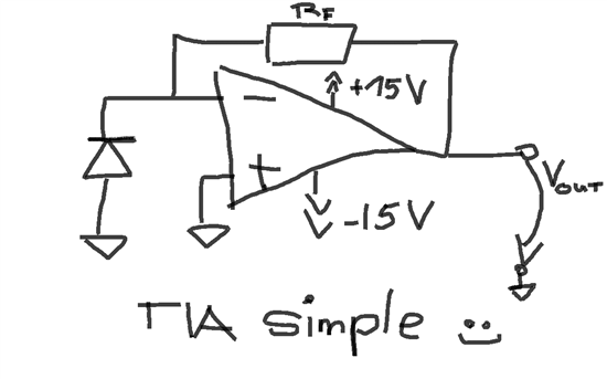
What I do not know: Is the Input Offset voltage also amplified through Feedback resistor Rf or not? Right now I would say it is not. Since I do not measure it at my amplified Output.

As I read the Input bias current really is present amplified at the Output, now I did measrue 2 different OpAmps, both dual channel, one is the good old JFET Input ( for low bias current ) TL062, the other one is the modern bipolar ( for low Offset voltage ) OPA2277 with a lot more bias current.

Now I do use different Feedback resistors, like 10k, 100k, 1M, I would suppose I get a different Output voltage each time in accordance to my bias current times Feedback resitance. But I do actually not measrue it.

Ouput voltage I do measure in DC with an modernreliable :) agilent multimeter, i can measrue to 0.001mV, although lets say it will measure 10µV stable, I would think I at least should measrue the 1Mohm bias current amplification, but I cannot see it yet.

So this is where theory and Praxis is striking me once more :)

To say on my Input I use a BPW21, that is a Si-Photodioe (so it can measure visible light )  with a really big active area ( around 580 pF capacitance ). Maybe this is also my Problem in the measruemtn, since this is a really big Input capacitance, hadnt time to evaluate this.

Both the OpAmps I supply with a linear power supply +- 15V, aha and now that I think of it, I do not use any blocking caps ( 100 nF), but honestly I do not expect any outcome changes if I would use them, since it is a linear power supply , but who ever knows...

So this is where I am so far, now I would like to hear from you, feel free to share your Points of view, I would prefer rather someone who actually works with it, in regard to solder iron and PCBs, than theoratical views, I do have a lot them :) and honestly the solder iron is my Spice, too :)

Best wishes,

seb

  • Seb,

    I don't uses photo diode often, but TL062 is mine. 
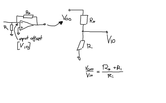
    VIO will be present at inverting input. DC gain of VIO is 1+RF/RI. RF is easy. RI is the diode. If was an idea current source then VOUT would be same as VIO. A diode at a couple mV should be a very high resistance.

    Input bias current is a DC error adding a resistor to the other input lower error to IIO. Resistors do have a thermal noise to consider.

    Others may provide more useful information.

  • yeah i like paint :)

    And thanks for the first part, I do understand the output offset now, as long as the diode resistance is a lot bigger than the feedback resistor it doesnt play a role, but as soon as the feedback resistor gets bigger, which is the case sometimes, it will raise. What would be interesting now, how it reacts when biasing the photodiode to minimize the capacitance, how low does the diode resitance get?

    Ron Michallick said:
    Input bias current is a DC error adding a resistor to the other input lower error to IIO. Resistors do have a thermal noise to consider.

    That sentence doesnt even sound english to me , let me translate that to what I think you want to express :)

    If I add a resistor to the positive input, which is almost identical to Rf || Ri, which should be a value around Rf, since Ri is way bigger than Rf, then the dc error current into the positive and negative input of the OpAmp should be almost identical, so the bias currents will cancel each other out. So long goes the theory.


    What you already mentioned the high value resistor adds some thermal noise ( johnson noise ) to the whole circuit, which is generally not recommended, and I never saw an actual circuit which had this bias current cancelation ( I mean a circuit actually in production and beeing sold to costumers ).

    But my actual question would still be: Ho does the output see the input bias current error? I think it will se it with a DC gain of the value Rf, just like the transimpedance amplifier works.

    And how about all the other parameters, are the voltage noises tranfered with a gain or without gain, what about the current noises and so on, any ideas will get appreciated :)

    Have a nice day.

    Seb

  • Seb,

    The DC voltage error from IIB is IIB * Rf. Current noise should scaled with Rf (In*Rf). Noise voltage gain should be near 1.