This thread has been locked.

If you have a related question, please click the "Ask a related question" button in the top right corner. The newly created question will be automatically linked to this question.

INA2143 instability

Other Parts Discussed in Thread: INA2143, OPA548, INA143, INA106

Hello,

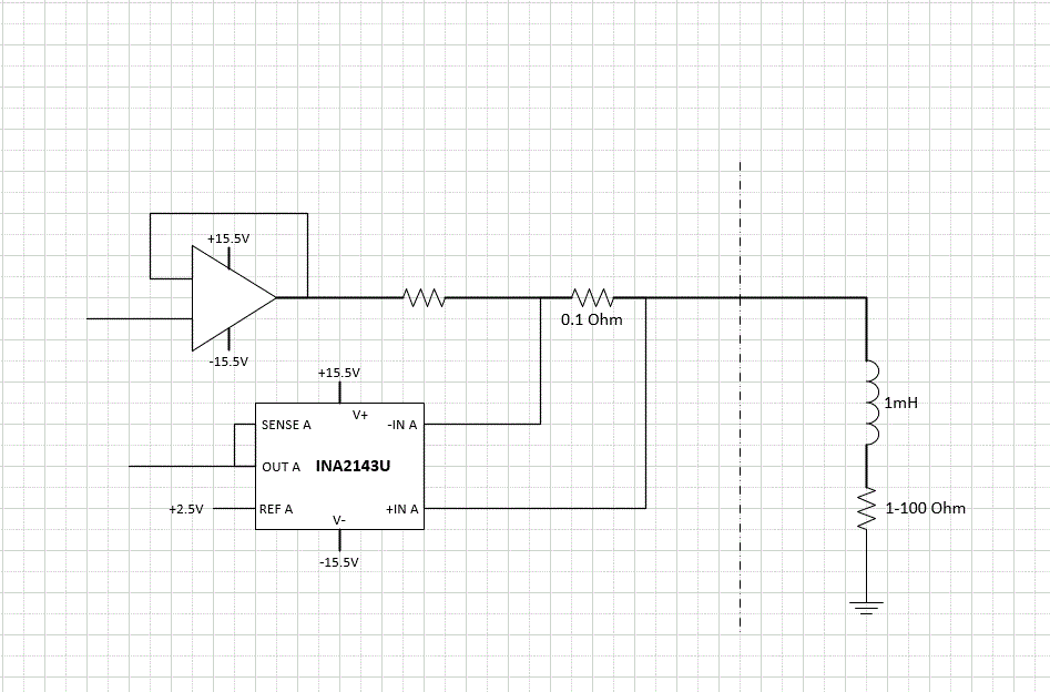
I am using a INA2143U for a current measurement circuit. (sense resistor = 0.1 Ohm, load = 1mH, 10 Ohm).

Measurements show that the INA2143 is not linear: for frequencies higher than 10kHz there are large spikes and dips in gain.

-The specific frequencies of these spikes and dips depend on the inductive load: at 2mH the frequency is cut by half

-The frequency is independent of the resistive load.

-If a purely resistive load is applied, the INA2143 is linear.

-The load is not oscillating with any (parasitic) capacitance in the circuit: it is tested by removing all capacitors that could cause an oscillation

Question:

Are there any preceding occurrences of this behavior documented?

Is the INA2143 unstable or is it incompatible with this circuit/load?

What could be done to stabilize the INA2143?

  • Hello Tim,

    It's fairly uncommon to use the INA devices like the INAx143 to drive large inductive loads so we don't have any preceeding cases of this documented to share with you.  What type of load is the INA driving that results in the 1-2mH of inductance?

    We'll perform some simulations on the circuit to understand what's causing the issues.  Could you please share a full schematic for us to review and use to build our simulation circuit?   

  • Hello Collin,

    When I mentioned a load inductor, I meant a load of the linear end-stage, on which the current measurement is performed, see picture below. It determines the input impedance of the INA2143.

    The end-stage input voltage can vary between -14V and +14V and currents between -2A and +2A are to be measured. Stability measurements are performed using a small-signal sine wave.

    Tests performed that had no influence on the behavior:

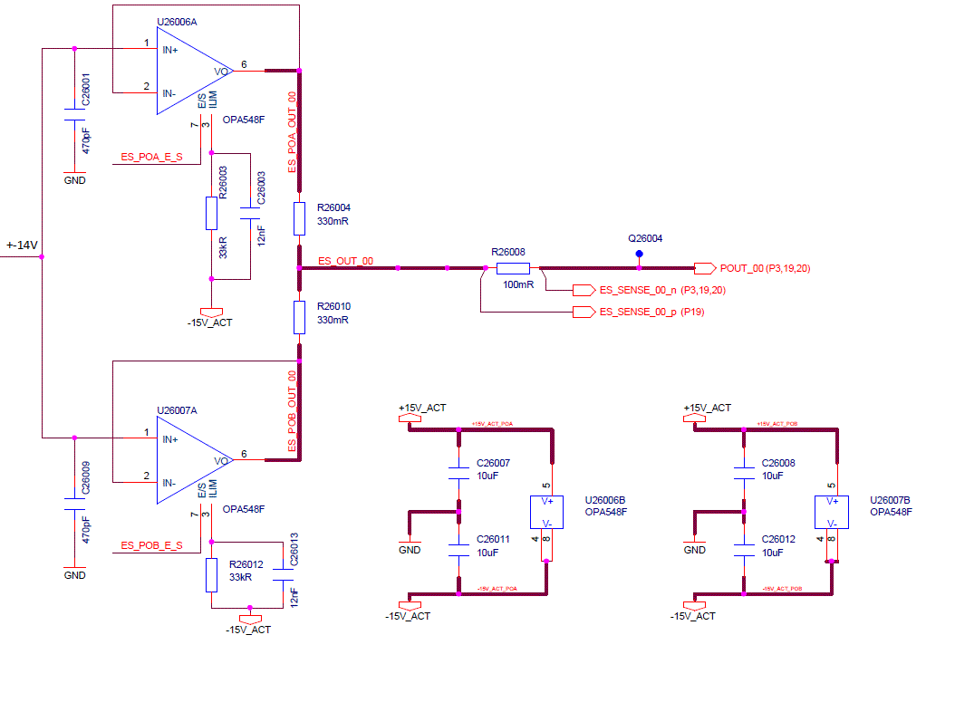
    -remove R26010 to see of the two OPA458 in parallel cause instability.

    -Remove C26001, C26003, C26009, C26013, C19033 to detect inductor-capacitor oscillations

  • Hello,

    Thanks for sharing this portion of the schematic.  Could you share the exact load that is placed on the "POUT_00" net?  

    Which net are you measuring the instability on?  Have you confirmed that the output of the OPA548(s) is not the source of the oscillation?  Both or one of the OPA548 devices could be oscillating depending on the output load and how it interacts with the output impedance of the amplifiers.

  • Hello,
    The load of POUT_00 is 1mH, 3.5 Ohm. The resistance can vary, but this is the typical value.
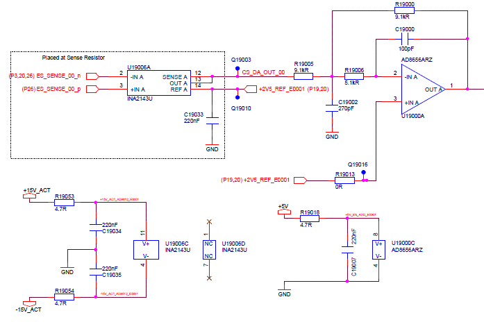
    for The OPA548: I measured at the input (voltage over R26008) and the output (CS_DA_OUT_00) of the INA2143: the input is as expected but the output is unstable. Also, I tested with 1, 2 and 4 OPA548 in parallel on multiple setups and the behavior is always exactly the same. If the OPA548 is the cause, it would imply that the frequency would change for more OPA548 in parallel.
    Regards,
    Tim Meyskens
  • Hi Tim,

    We've been working on evaluating the stability of the OPA548 and INA143 in the circuit and have not been able to determine where the oscillations you're describing are coming from.  Could you please share an image of a transient or ac frequency domain response of the circuit so we can see the issues that you're seeing?

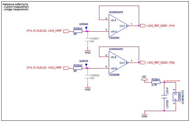
    Also, please show us the schematic of what the 2nd channel of the INA143 is doing and also how the +2.5V reference voltage is being generated.  Any chance that the +2.5V reference circuit is not stable and causing the issues you're seeing?

    Finally, although the oscillations don't appear to be related to the OPA548, we still recommend that an output snubber network is included any time the output of a power amplifier is required to drive complex loads.  In parallel to the suggestions above would you try adding the output snubber to the OPA548 outputs to cure any local output stage oscillations?

  • Hi Collin

    The image below shows the input and output of the INA143. due to a feedback loop the input in this image also shows the oscillations. There has been an open loop test, but no images where saved.  I will repeat the open loop test to make a proper transient image.

    A: voltage over sense resistor (x10)

    B: output voltage of the INA143

    the 2nd channel is used for a 2nd end-stage. the circuit is identical. is these tests the 2nd end-stage is disabled.

    the 2.5V reference should be stable: the decouple capacitor C19033 has been removed and nothing changed. However, it is something to look into. I will check this in my next measurement. I will also add a snubber .

    Regards,

    Tim Meyskens

  • Hello Tim,

    Please keep Collin as main contact. I merely wanted to suggest an additional test to narrow down the options were the oscillation might come from.


    Have an open loop configuration (no INA2143 signal, so remove R19005 for example) and capture a step response. Keep in mind to stay in the linear range of the system. The point here is to look for any ringing and frequency of it. This way you can test the interaction between load and driver without the INA2143. Please share the plot and we could additionally work from here.

  • Hello,

    Frank, thanks for your comments.  Based on the "B" measurement results there's something very strange going on with the INA143 circuit so I agree that we should try to isolate the INA143 from the other elements in the circuit to figure out what's going on.

    Tim,

    Thanks for sharing your results this is helpful.  First, the input of the INA143 circuit (Measurement "A") shows about 5dB of gain peaking which would indicate that the output of the OPA548 circuit only has about 30-35 degrees of phase margin which is lower than the 45 degrees (2dB gain peaking) we typically recommend for production systems. Frank's comments can be applied to the OPA548 circuit as well and we recommend that you disconnect the INA and verify through transient step response testing that the OPA548 circuit is stable before releasing this system to production.  Small-signal transient overshoot less than 25% correlates to phase margins greater than 45 degrees.

    Second, the AD8656 reference buffer circuit will eventually need to be redesigned.  There's no way that the op amp can directly drive 220nF of capacitive load and remain stable.  I know you've removed the load capacitor from the channel you're testing, but make sure it's removed from both channels or there could still be issues from the other channel oscillating.

    Third, it looks like the AD780 circuit could significantly benefit from adding another capacitor to the "TEMP" pin to reduce the noise performance as described on page 6 of the AD780 datasheet.  For a 100uF output capacitor it looks like around 47nF is recommended.

    Regarding the INA143 output, I've pasted an image of the expected closed loop response of the INA143 below.  As you can see the expected gain response is very flat over frequency up to 100kHz.  The results you shared show both high-pass and low-pass filtering effects (along with severe gain peaking) and I can't find any reason based on your schematic that we would see such results.  

    As Frank suggested could you repeat the measurements without the AD8656 filter (U19000A) in the circuit to understand if the circuit is somehow interacting negatively with the INA143? 


    Let us know what you determine through your testing.

  • Hello Collin,

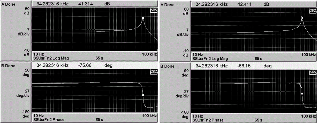
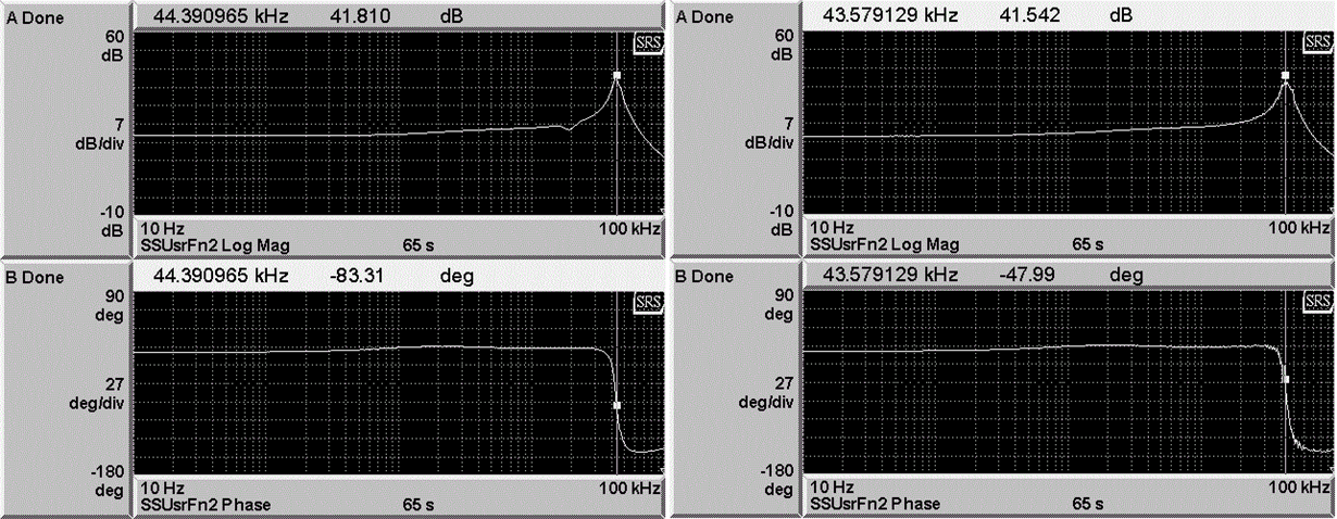
    -I performed some measurement, and at least the oscillations no longer seem random. there is a clear oscillation frequency.

    the transfer function of the INA143 is shown below:

    closed loop, 1.15mH                                                                                                     open loop, 1.15mH

    closed loop, 0.78mH                                                                                                       open loop 0.78mH

    left: closed loop. right: open loop (the loop is digitally cut on an FPGA)

    top: 1.15mH load. bottom: 0.78mH load

    A: magnitude. B: phase.

    -the circuit is stable with enough phase margin. the 5dB peaking is caused by the oscillation.

    open loop response: GM=8.99dB, PM=54˚, BW=9.59kHz

    -I agree that the 2.5V reference buffer should not drive a 220nF load, I must have overlooked this. However I did measure the 2.5V reference

    and it is stable. there is also no measurable correlation between the 2.5V reference voltage and the current through the load (I measured the 2.5V with a spectrum analyser while adding a sine wave at the OPA548 input).

    I replaced C19033 by 47pF (on both channels), which should be ok. It has no influence on the behavior.

    -I also checked the supply rails, they are stable and there is no measurable correlation between the supply voltages and the current through the load.

    regards,

    Tim Meyskens

  • Hi Tim,

    We appreciate your measurements, however we can't conclude yet that this is caused by the INA2143. In the measurements there are to many influences which could play a part.


    To me the step response test (without INA2143) would be still valuable.


    Maybe I should explain a bit more on my thoughts here as well. The OPA548 in non-inverting configuration is less stable then an inverting configuration. Secondly the high inductive loads have planty of windings which cause inter winding capacitance. Looking at your measurement results this is in the range of ~18nF. Both your measurement confirm this actually. An impedance plot over frequency of the load impedance (only the load impedance) might give more insight into this.


    Lastly I can only restate again that we need to narrow down the number of sources that could cause the oscillation you are seeing.


    Finally I'm curious about your actuall issue, as you mentioned the circuit is stable after all.

  • Hi Frank,

    I agree on the step response, I will do this today.

    We have tested all parts of the circuit and found that only the INA2143 has the oscillation in its transfer function. We can at least conclude that the INA2143 is part of the problem. Also, the INA2143 transfer function is the only test where a clear oscillation frequency is observed. All other measurements  give conflicting data.

    I know it looks like an oscillation with a ~18nF capacitor, it was the first thing I tried to find. I removed every possible capacitor and there is no way the parasitics on the circuit could add up to 18nF. I measured the capacitance of the load, and it is in pF range. Further, the tests have also been performed with a digital load with the same results. Also, if the inductance is oscillating with a capacitance somewhere, it would not show so clearly in the INA2143 transfer function. this could only happen when the parasitic capacitance of the INA2143 is 18nF, which would be really high. The current and voltage of the load are not oscillating (in open loop), only the output of the INA2143.

    At some point I also considered delay between ES_SENSE_00_n and ES_SENSE_00_p, but the lines are too short to cause problems at these frequencies.

    the power supplies, nor the 2.5V reference show any measurable reaction to the oscillations.

    As far as I can see, the only conclusion left is that the INA2143 cannot handle a 1mH input impedance. Either it becomes unstable, or the combination of parasitic capacitance, (internal) resistance and input inductance causes oscillations.

    I could try to ad a small capacitor between ES_SENSE_00_n and ES_SENSE_00_p. if the INA2143 is indeed unstable, this could improve the behavior.

    As for the actual issue: the circuit is indeed stable for this application, but a wide variety of loads is required ranging from 0.1 Ohm to 100 Ohm and 0 H to 2mH (or higher if possible). I could never explain this issue to a customer. Also, I had to decrease the bandwidth to get the stable behavior, lower than currently specified. Without the oscillations I would meet the specifications. If there is no possible solution, so be it. I will try to work around it, but it is far from ideal.

    Regards,

    Tim Meyskens

  • Hi,

    I have some more test data:

    -I noticed that the transfer function pictures are accidentally inverted: there is actually a dip in gain and the phase goes from 0 deg to +125 deg.

    -I added a 10nF capacitor between ES_SENSE_00_n and ES_SENSE_00_p: no change in behavior.

    -I added a capacitor between ES_SENSE_00_p and ground:

    added capacitance 0 10nF 20nF
    dip frequency 33kHz 39kHz 48kHz

    the more capacitance is added, the higher the frequency of the gain dip. Also, with more capacitance the dip is less steep.

    regards,

    Tim Meyskens

  • Hi,

    I did the open loop step response: there is no ringing.

    There is a small voltage overshoot of 0.1V (2V step, 500kV/s), but that is to be expected: 

    regards,

    Tim Meyskens

  • Hi Tim,

    I'm running out of ideas and hope that Collin has some additional comments.


    One of my thoughts:

    • could you swap the inputs of the INA2143 and see if this changes things (you may need to invert some results depending how you test, or your measurement equipment processes it)
    • Personally I'd still try to look at the OPA548 as well
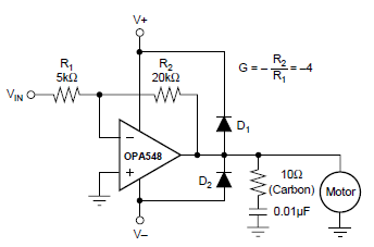
      • try insert feedback loop/resistor of OPA548, it has no damping at all, try 100-1kOhm range and look for changes
      • inverting mode looks still better choice if you ask me, set gain -1 as in below picture but then R1=R2= 1k-5kOhm, look for changes in oscillation freq. Keep in mind to add the series resistors to parallel the OPA548, however for the test a single OPA548 might be okay too.

  • Hello,

    I am also unsure where the issue in this circuit is coming from.  Were the phase-margin measurements performed on the entire system, or just the INA143 portion of the circuit?

    We're continuing to investigate this issue and will report back when we have an update in the next day or two.

  • Hi,

    the phase-margin measurement is performed on the entire system.

    I swapped the inputs of the INA2143 as Frank suggested and got some curious results. I do not know if they are reliable though: right after the test the INA2143 broke. I think I damaged one of the pins, I am currently waiting for spare parts.

    open loop transfer function INA2143 with swapped inputs.

    (To answer the question in advance: no the result is not inverted, I double checked)

    I will do more tests as soon as I can.

    Regards,

    Tim Meyskens

  • Hi,

    I did some measurements while bypassing the existing circuit layout. This to check if the layout adds delay, filters the input,...

    There was no difference in result.

    Regards,

    Tim Meyskens

  • Hello Collin,

    do you have any progress on the issue?

  • Hi,

    I added a feedback loop resistor of 470R to the OPA548 as Frank sugested, there was no difference.

    As for inverting mode: I could try it, but the topology was chosen because it adds no gain error to the end-stage.

    If I were to use the OPA548 in an inverting circuit with 0.1% tolerance resistors it is likely that the gain error becomes too high.

    Also, the difference between the two opamps would be higher, resulting in more losses and a higher OPA548 junction temperature. The OPA548 temperature is one of the most crucial limiting factors in this design.

    regards,

    Tim Meyskens

  • Hello Tim,

    Thank you for your additional testing.  We've been able to confirm that the issue you're having in your schematic appears to be related to the topology of the circuit itself and not the INA143.  As you can see in the figures below we've simulated your circuit with the INA143 and confirmed there is very strange AC transfer function response when the inductor is placed in series with the 100mΩ shunt resistor. 

    INA143 circuit with 1.15mH inductance in series with the 100mΩ


    Results with 1.15mH inductance:


    Results with input inductance removed:


    To show the effects are not related to the INA143 itself, but the actual topology of the circuit we created a simplified model of the INA143 using a single –pole open-loop gain (Aol) and 120Ω open-loop output impedance (Zo) as shown below:


    Results with the 1.15mH input inductance:


    Results with inductance removed:

    What’s happening at high frequencies in this circuit is that the op amp runs out of loop-gain and all that’s left in the circuit is the open-loop output impedance and a low differential gain. This results in an impedance divider that causes the system gain to appear to increase over frequency. The gain of the INA143 is not increasing but the apparent system gain does increase because of the impedances that remain in the system once the op amp is out of loop-gain.

    The simulation below shows a simplified version of the circuit where the inductor has been replaced with a changing resistance to mimic the change of the inductor impedance over frequency (XL = 2πfL). The op-amp open-loop gain (VCVS3) has been reduced to 1V/V to show the effects at high frequencies. As shown in the simulation results the Vout/Vin (Gain) transfer function increases as the impedance of the inductor increases.

    If the amplifier still has loop-gain it will regulate the Vout/Vin transfer function to the expected 10V/V gain. This is shown in the simulation file and results below where the Aol (VCVS3) is left at 1M V/V and the dominant pole is removed to prevent the loop-gain from decreasing over frequency.


    In summary, this is a system level issue that will affect any real amplifier that has a non-zero output impedance and frequency limited open-loop gain / bandwidth. Higher bandwidth products will have more loop gain at lower frequencies which will push the issue out in frequency. This can be seen in the simulation results below where the unity-gain bandwidth of the simple single-pole amplifier has been increased by 10 times. As you can see the unwanted impedance interactions have been pushed further out in frequency.


    Thank you for your patience while we were understanding the operation of this circuit which was not immediately apparent.

    Here are the simulation files used for this analysis.  Please let us know if there are any additional questions.

     Basic_SCH_Positive.TSC

    Discrete_+DiscreteAol.TSC

    High Freq Operation Rev A.TSC

  • Hello Collin,

    Thank you for the analysis, this is really helpful.

    I am trying to find a difference amplifier with a higher gain/bandwidth that could replace the INA2143.

    However, as far as I can see, The INA2143U is the only one that matches my specifications.

    Component

    Condition

    required

    INA2143U


    Gain


    10

    0.3%

    10

    0.05%

    Reference gain


    1

    0.3%

    1

    0.05%

    CM Input voltage range

    Power supply ±16V, Vref 2.5V

    -14.7V to 14.4V

    -16.6V to 15.6V

    Power supply ±15V, Vref 2.5V

    -14.7V to 13.4V

    -15.5V to 14.6V

    BW


    2MHz

    150kHz

    CMRR


    80dB

    86dB

    Output noise


    100 nV/√Hz

    45 nV/√Hz

    Offset


    ±0.4mV

    ±0.25mV

    Supply


    ±16V

    ±18V

    Are there any components you can propose? 

    I also tried instrumentation amplifiers, but I had the same problem.

    Regards,

    Tim Meyskens

  • Look at INA106. If you cannot get what you need you can do it with an op amp and a resistor network that has ratio matched resistors for best common mode rejection ratio.