This thread has been locked.

If you have a related question, please click the "Ask a related question" button in the top right corner. The newly created question will be automatically linked to this question.

IVC102 inexplicable jump when S1 opened after integration

Other Parts Discussed in Thread: IVC102, SN74LVC2G17, MSP430FR5969

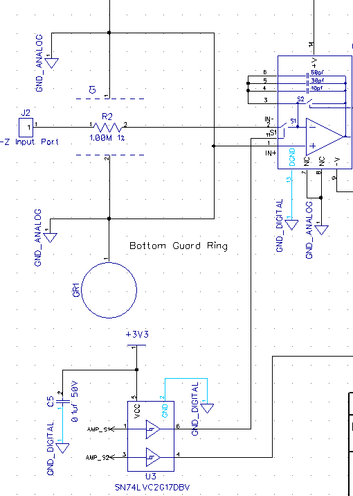
Using the IVC102 as recommended (data sheet page 7 Figure 3a), and with nothing on the IVC102's input (left floating within its guard ring), Testing is now being performed to characterize drift.  This was an issue that we found on a previous board design and so for this one we improved guarding and took extra care to eliminate/reduce any leakage paths possible.  No feedback resistor is used here.  We want to eliminate any noise.


The test follows this sequence:

  • open inverting input switch (S1)
  • close reset switch (S2)
  • wait 1 second
  • open reset switch
  • close input switch
  • integrate for 30 seconds
  • open input switch
  • read value
  • repeat

Before we start the integration and with the reset switch CLOSED, we see about +0.0005 V at the output. 

With 100pf selected (default for my board) the drift amounts to -0.025V every 60 seconds.  This seems reasonable, and when I change capacitance to 40pf, the rate is consistent, rising to -0.047V/60 seconds.

There are two values I don't understand just yet.  Perhaps a TI Engineer can chime in here:

  1. Following integration, we OPEN the input switch (leaving the reset switch unchanged (open)),  At this point, the output value suddenly changes from the expected -0.025V to -0.038 V.  Why?  The data sheet tells us that opening S1 will leave the integration value on the internal capacitors until we reset. 
  2. Drift is greater when we perform our testing with S1 OPEN (not connected to the outside).  We see -0.058V every 60 seconds when we integrate in this condition.  I'd expect a higher drift rate with S1 CLOSED as outside influences come into play.  My guess is that the outside influences are opposing the higher (internal?) drift rate.


A bit of information on how S1 and S2 are interfaced: I'm using a TI SN74LVC2G17 (dual Schmitt-Trigger buffer) between my microprocessor (MSP430FR5969) control lines for the two switches and the IVC102.  This is a design change which assures signal purity and noise immunity for the switches.

Also, digital and analog gnd is joined at an interface connector on the preamplifier board and the switch lines are guarded by digital gnd, per the data sheet (just in case).

Here's a snippet:

  • Hi Mark,

    I spoke with my colleague the IVC102 designer this morning. He was able to provide me some insight into your questions:

    1. Following integration, we OPEN the input switch (leaving the reset switch unchanged (open)),  At this point, the output value suddenly changes from the expected -0.025V to -0.038 V.  Why?  The data sheet tells us that opening S1 will leave the integration value on the internal capacitors until we reset.

      This behavior is due to charge transfer when is S1 is switched from closed to open. Some characterization data we have indicates that the charge Q, is about 1.7 pC, with no external capacitance connected to the IVC102 -In input. You are using the 100 pF for the integration capacitance. When the switch S1 changes state, the charge injection current results in the output voltage change; V = Q / C = 1.7 pC / 100 pF = 17 mV. You are seeing a change of 13 mV so the charge transfer is a little lower for your device.

    2. Drift is greater when we perform our testing with S1 OPEN (not connected to the outside).  We see -0.058V every 60 seconds when we integrate in this condition.  I'd expect a higher drift rate with S1 CLOSED as outside influences come into play.  My guess is that the outside influences are opposing the higher (internal?) drift rate.

    The drift based on the numbers you have provided is 58 mV in 60 seconds, or 0.96 mV/ sec. This drift is from the IVC102 integrating the input current when S1 is open. This current is calculated from: I = C (∆V /∆T) = 100 pF (0.96 mV / sec) = 96 fA. The input current can be much higher than this. I suspect that when S1 is closed the leakage current is actually in the opposite direction of the input bias current - in this case, resulting in a lesser total current and lower drift rate.

    Regards, Thomas

    PA - Linear Applications Engineering


  • These explanations jive with testing on three prototypes build using the IVC102. Thank you.

    We hope to resolve currents in the order of 10^-12 A with a 30S integration period.