This thread has been locked.

If you have a related question, please click the "Ask a related question" button in the top right corner. The newly created question will be automatically linked to this question.

About whisker (negative voltagfe) of OPA549 output

Guru 19485 points
Other Parts Discussed in Thread: OPA549, TINA-TI

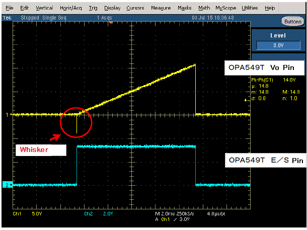
When 9-pin(E/S) are made Low⇒High and OPA549 output is done in Disable⇒Enable, the negative voltage whisker is output.
※Waveform is attached below

Please let me know about below.

・When OPA549 is Disable, is the internal circuit down which -15V is flowing here?

  ⇒When there is information of internal circuit, please give me.

・Is there a measure?


【Additional information】

・Supply voltage:±15V

・When -VS is changed to GND from -15V, it becomes good. (No whisker)

・Control of E/S is High/Low signal of MCU into buffer IC.

   ⇒The amplitude of whisker is depend on off/on timing.   (Max:0.6uS width/ -5V.)

・Even if a loop of OPAMP is cut off, it occurs.

・The customer request, the negative output is bad.

~Customer Information is below~

  • What is end Application

     ⇒Portable healthcare

  • What is subsystem part is used on?   

            ⇒±15V current output AMP

  • Part input signals: amplitude
  • Part output load: dynamic
  • Power supply:LDO


Best regards,

Satoshi

  • Satoshi,

    Your waveform failed to load-please use Insert/Edit media button to attach it (btw, what do you mean by whisker?)

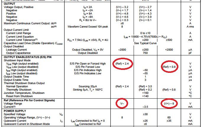
    All REF's and Enable/Disable treshold voltages are referenced with respect to the power supplies - see below - make sure you do not violate them.

    Therefore, for +/-15V supplies, the REF pin must be connected between -15V and +7V but for  +15V/0V supplies REF pin must be beween 0V and +7V.

    The output is enabled for E/S at or above VREF+2.4V and disable for E/S pin between VREF and VREF+0.8V

  • Dear Marek Lis-san

    Thank you for reply.

    And, sorry for waveform failed.

    Waveform is attached again, please see below.

    Best regards,

    Satoshi

  • Dear Marek Lis-san

    Customer information is updated below.

    【Additional information】
    ・Supply voltage:±15V
    ・Input voltage(4 pin):+3.7V
    ・Vref:GND
    (Is Vref necessary to -V?)
    ・Output capasitor is nothing

    【Additional question】
    ・Is there internal circuit (of negative voltage rail)?
    ※Customer wanto to understand internal circuit of negative voltage line at disable.
    ・When there are a problem and a correction point, please let me know.

    Best regards,
    Satoshi
  • Satoshi,

    In order to assist you, it would be very useful to show the circuit configuration as well as the detailed information on the input signal.  Looking at the waveforms, I can only speculate that OPA549 is being used in the gain G=+3.  If so, with the negative supply voltage at GND, the output seems to be initially pushed against its negative rail resulting in a non-linear operation of the output stage – the lower output stage transistor is turn-off.  As you enable E/S pin, it takes few nanoseconds for the output to come alive which results in the negative spike (whisker) at the output.  In case of the negative supply of -15V, the output most likely is still driven to 0V (and not -15V) and thus stays within OPA549 output linear range; in such case, there is no whisker since the lower output transistor does not need to recover from being turn-off.

    As I wrote before, for +/-15V supplies, the REF pin must be connected between -15V and +7V but for +15V/0V supplies REF pin must be between 0V and +7V.

  • Dear Marek Lis-san

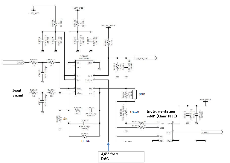
    For additional information, circuit diagram is below attached.

    ・Customer evaluated that Off⇒On speed (timing) made bery slowly, but negative noise (whisker) is occured.

    ・We simulated TINA-TI for OPA549.

     When Off⇒On, positive noise is occured.

     And, when feedback resister set large value (more than 15kΩ),  negative noise (whisker) is occured.


    I think that noise is depend on device spec.

    Is there any idea of reduce noise?


    Best regards,

    Satoshi

  • We need to do a complete analysis on this circuit for phase margin to ensure we are very stable as turning on into a marginally stable circuit will cause undesirable effects. Please answer the following and I will perform a loop gain analysis for stability.
    1) Is R4005 (2K) tied to ground and used as shown in the circuit schematic?
    2) Need Instrumentation Amp part number as its closed loop BW is in the feedback path.
    3) Is there a specific closed loop BW the customer needs to control current in the load?
    4) Is the load pure resistor of 30 ohms or is it inductive, capacitive?
    5) Is the input signal only DC? If not amplitudes, frequencies, duty cycles of input signal.
    6) Power supplies on Instrumentation Amplifier?
    7) Is instrumentation amplifier powered on during enable/disable of OPA549?
    8) What is the system goal for this circuit? To turn on/off output of OPA549 as high impedance? Or is zero output okay when OPA549 is "off"?
    9) In general enable pins on op amps are not without some transients on output since you are changing amplifier operation from open loop to closed loop and depending upon the turn-on bias of the output stage it may or may not spike negative. I would not rely on turn on behavior of one part as over process and temperature that behavior may change.
    10) Where is Tab of OPA549 connected to?
    11) Is OPA549 heatsinked? If so what is thermal washer between Tab and heatsink?
  • Dear TIM-san

    Thank you for information.
    I answer a confirmation matter below.

    -------------------------------------------------------------------------------
    1) Is R4005 (2K) tied to ground and used as shown in the circuit schematic?
    ⇒Yes, R4005 connect to GND.

    2) Need Instrumentation Amp part number as its closed loop BW is in the feedback path.
    ⇒Device name is AD8429ARZ (ADI).
    www.analog.com/.../AD8429.pdf

    3) Is there a specific closed loop BW the customer needs to control current in the load?
    ⇒No, customer is not need specific closed loop BW.

    4) Is the load pure resistor of 30 ohms or is it inductive, capacitive?
    ⇒Load pure resistor

    5) Is the input signal only DC? If not amplitudes, frequencies, duty cycles of input signal.
    ⇒Input signal is Ramp signal of 0~3.5V.

    6) Power supplies on Instrumentation Amplifier?
    ⇒±5V

    7) Is instrumentation amplifier powered on during enable/disable of OPA549?
    ⇒Yes.

    8) What is the system goal for this circuit? To turn on/off output of OPA549 as high impedance? Or is zero output okay
    when OPA549 is "off"?
    ⇒High impeadance.

    10) Where is Tab of OPA549 connected to?
    ⇒Tab is open.

    11) Is OPA549 heatsinked? If so what is thermal washer between Tab and heatsink?
    ⇒Yes. Heatsink is connecting OPA549 in between the isolation seat.
      ※Heatsink ⇔ Isolation sheet ⇔ OPA549
    -------------------------------------------------------------------------------

    Best regards,

    Satoshi
  • Dear TIM-san

    When you find other worrisome points and confirmation items, please let me know.
    I'll confirm immediately.

    Best regards,
    Satoshi
  • See attached for my analysis based on a long discussion with IC Design and some of my own analysis.  Let me know if any questions.

    OPA549 Negative Whisker.pptx

  • Dear Tim Green-san

    Thank you for strong advice.

    Please let me confirm 2-points below about material.

    ①What changes with changing it to-5V from-15V?
    (Why doesn't negative glitch occur any more?)

    ②On OPA549 datasheet-P3, Output Voltage(Negative) is "(V-)+1.4 at Io=-2A".
    I think that, when (V-) connect to GND, Output drop to +1.4V.
    Is it right?
    (Addition, when Input set to 0V, Output is 0V,too.)

    Best regards,
    Satoshi
  • Please let me confirm 2-points below about material.

    ①What changes with changing it to-5V from-15V? 
    (Why doesn't negative glitch occur any more?)

    Answer: By running OPA549 from +15V, -5V you reduce the negative supply so I would think (not guarantee) that the glitch would reduce since again I assume turn on will spike negative since negative output stage has a local feedback loop. Lower negative voltage should correlate to less glitch.

    ②On OPA549 datasheet-P3, Output Voltage(Negative) is "(V-)+1.4 at Io=-2A".
    I think that, when (V-) connect to GND, Output drop to +1.4V.
    Is it right?
    (Addition, when Input set to 0V, Output is 0V,too.)

    Answer: Single supply is NOT recommended because your Vin voltage goes from 0V to 3.5V and you need OPA549 output to go from 0V to about 10V.  Single supply will not let the output guarantee to go below 1.4V at 2 amps sink.