This thread has been locked.

If you have a related question, please click the "Ask a related question" button in the top right corner. The newly created question will be automatically linked to this question.

XTR300 gets hot

Other Parts Discussed in Thread: XTR300

Hi, folks

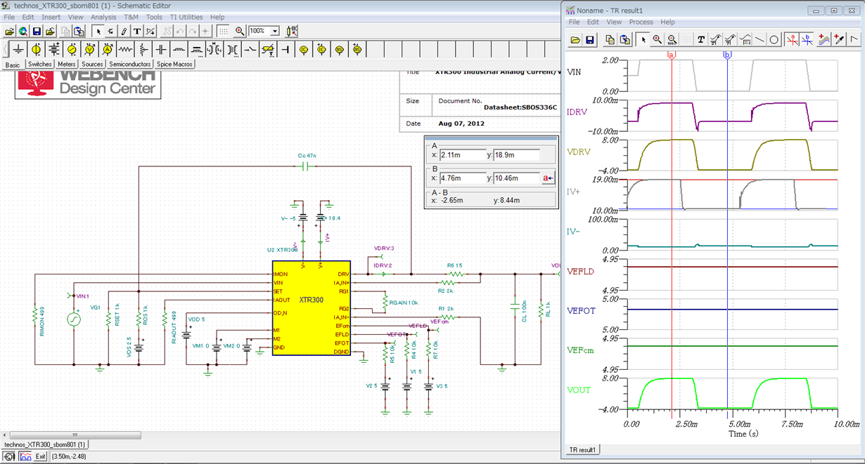
In following schematic, the case temperature of XTR300 will be 55 degC.

The consumption current is only 18.9mA, so Tj should be around 42.5degC, Tc should be around 32degC.

I am wondering why the XTR300 gets hot.

Could you review schematic and let me know if there are findings?


  • Hello,

    Are you sure you've configured the circuit the same way the customer has?  It would appear that with an input voltage swing of 0-2V, a Vos voltage of 2.5V and Rset and Ros = 1k, the output swing of this circuit will be from +7.5V to -12.5V.  I've shown this in the simulation file and results below when using +/-20V supplies.  

    A +7.5V to -12.5V output swing is outside of the power supply range with V+ set to +19.4V and V- set to -5V.  Do we have the circuit configured correctly?  If so, the product may draw slightly higher currents in conditions where the output is fully saturated. such as when it tries to drive to -12.5V but is limited by the -5V supply voltage.

  • Collin,

    Thank you for your reply.

    I confirmed with customer, but they saids that VIn will be 0-2V, but DC.
    I will let customer to use 0.4-2V based upon your suggestion, but there is still "Hot" problem when applying VIN=2V(DC).

    I am asking to review artwork, but could you tell me if there are another issues on schematic point of view?
  • Hello,

    With the circuit connections configured as previously shown, the customer would need to limit the input voltage to 0.7V - 2V to keep the output voltage within the supply voltage range of +19.5V / -5V. 

    Please get the artwork so we can review their PCB layout, we haven't identified any issues with the schematic besides the input/output voltage scaling issues described above. 

    Has the customer properly connected the PowerPAD on the bottom of the IC to the negative power supply potential (V-)?  The PowerPAD needs to be connected to a power plane capable of removing heat from the IC.  The thermal impedance specifications for the XTR300 are based on a PCB layout that properly removes heat from the XTR300 PowerPAD.  Information on this topic is provided at the end of the XTR300 product datasheet.  I've copied some of the information below. 

  • Collin,

    I will visit customer to do further check tomorrow, but BTW I could like to confirm VIN(Min).
    The spec sheet said that Vout swing range is (V-)+3V, in this case it will be -2V.
    So Vin should be above 1.05V, I guess. Am I correct?

    The simulation circuit is exact same as customer's circuit. (But I will double check with customer tomorrow.)
  • Hello Keiichi,

    The minimum input voltage is based on the power supply voltages of the XTR300 and has an absolute maximum rating of (V-)-0.5V to (V+)+0.5V. The rated input common-mode range is (V-)-3V to (V+)+3V. As long as the input remains within the power-supply voltages there will not be any damage to the XTR300 input pins.

    The output of the XTR300 should not be expected to swing any lower than (V-)+3V as you've stated. With a supply voltage of -5V, the output should not be expected to go any lower than -2V over the temperature range.
  • Hello Collin,

    Thank you for your reply.

    We disussed with customer, I am very sorry but our cusomer did not test under soldered board.
    I would like to ask you to discard these questions.

    Our customer wondering the XTR300 cosume about 10mA without load. I told simulation result and this value is quite reasonable.

    Also we told the estimation of Tj and Tc when load applied. Our customer decided to change board structure due to there is themal sensitive pastic currently near XTR300.
  • Hello,

    The quiescent current for the XTR300 is 2.3mA maximum at room temperature. Make sure the customer is accounting for the current delivered to the load as well as the monitor outputs.

    Also, the customer needs to properly solder the XTR300 to a PCB using the instructions in the product datasheet or the product may behave differently than expected.
  • Hello Collin,

    Attached is our simulation schematic. I added 1G ohm resistance as load. (Due to improving convergence)

    VIN=2V (DC). But this simulation result shows IV+ around 11mA.

    Could you tell me why it exceeds 2.4mA?

    XTR300_sbom801.TSC

  • Hello Keiichi,

    I have verified that there appears to be an issue with the XTR300 model that is resulting in the higher than expected quiescent currents.  As you can see in the simulation below with only 800nA of output current, the device still draws roughly 10.5mA of power-supply current.  This is not correct and the simulated power supply current should have been 2.4mA as stated in the device datasheet.