This thread has been locked.

If you have a related question, please click the "Ask a related question" button in the top right corner. The newly created question will be automatically linked to this question.

INA333: power up different behavior

Part Number: INA333
Other Parts Discussed in Thread: REF2030

Hello,

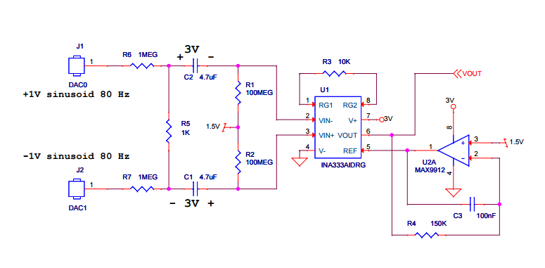
I have the following circuit:

SCHEMATIC1.pdf

At power up the two input capacitors are charged as shown in the attached schematic. A 1 mV sinusoid is applied at input using two DACs generating 1 V in opposite phases and a differential 1/1000 attenuator.

I have two INA333A marked as:

I333A

TI 5CK

C58V

and two marked as:

I333A

3CK

A5E5

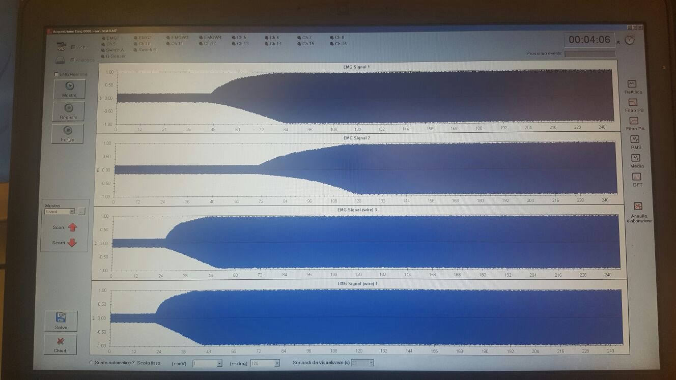
Their behavior at power un is shown in the photo: the upper two are the first mark type.

New Microsoft Word Document.docx

Is there any difference in the silicon release explaining such different behavior?

best regards,

Jacopo

  • Jacopo,

    It is impossible to read the details of vertical and horizontal axis in your scope picture but I may have some ideas for you to try.

    During power up sequence, and before the minimum power supply voltage of 1.8V is reached, INA333 circuit does not work properly and thus the output may be moving back and forth between the rails due to random nature of the input offset voltage.  

     I also see other potential issues with your circuit.  First, INA333 is a chopper instrumentation amplifier with the input bias current, IB, being dominated by short duration (few ns) current spikes caused by closing/opening of the front-end switches. The magnitude of the IB current spikes may be in tens of nV which combined with your R1 and R2, 100M, resistors converts those spike into voltage spikes with magnitude in several volts – I believe that is the cause of the voltage spikes seen on your scope picture.


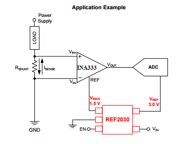
    Second, I do not understand why you drive the Vout of INA333 with 1.5V; if anything, in order to maximize the dynamic range of INA333 you would want to drive the V+ supply pin with 3V while driving REF pin with 1.5V – please take a look at REF2030 that specifically designed for this application (see below).

  • Marek,

    thank you very much for your fast feedback. Maybe this picture has a better resolution to see this sort of "amplitude modulation" on the input sinusoid:

    You have seconds on X axis and VOUT in mV on Y axis, with amplitude scaled to input. As you may see, VOUT reaches its full amplitude after seconds, but differently from a chip coming from the first lot to the second one. The big input capacitors magnify such phenomenon and my concer is to understand why units coming from different lots have such different transients.

    The circuit used to feed REF comes from a former version of the datasheet to get AC coupling:

    INA333 [TI] (ina333).pdf

    see Figure 37 on page 15.

    Best regards,

    Jacopo

  • Jacopo,
    As I said before, until the minimum power supply of 1.8V is met, INA333 will not operate under linear conditions and thus its output may not be controlled. For that reason, it's power-up Vout charactrisitcs may significantly vary not only from one wafer lot to the next but also between the units coming from the same lot.