This thread has been locked.

If you have a related question, please click the "Ask a related question" button in the top right corner. The newly created question will be automatically linked to this question.

OPA4188: Problem with Output offset of the analogic filters

Part Number: OPA4188
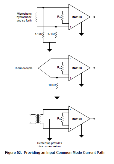
Other Parts Discussed in Thread: INA326, , OPA188, INA188, INA333

Hi

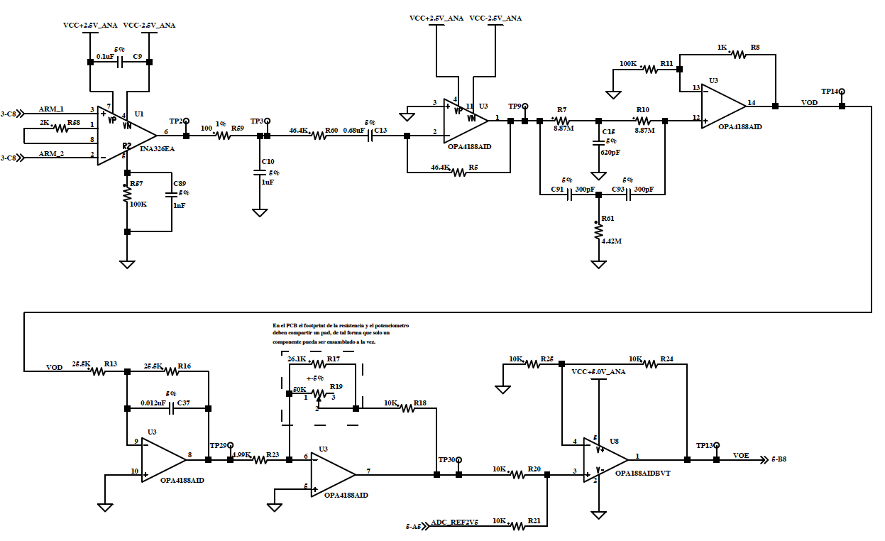
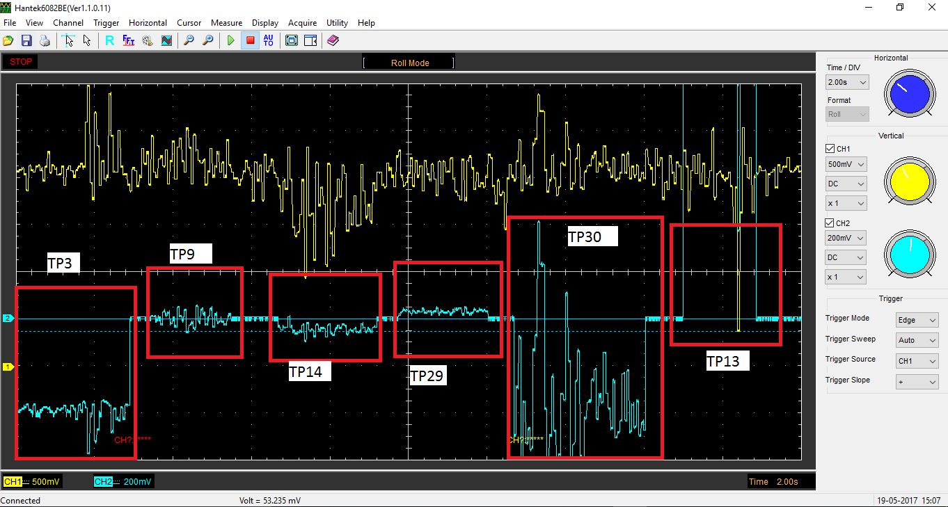
Command attached the stage of filtering that is being used (the POT (R19) was modified by one of 200K since the gain was insufficient). Yesterday I did some measurements on all the TPs of the filters and detected something. Using the oscilloscope in DC I saw this:

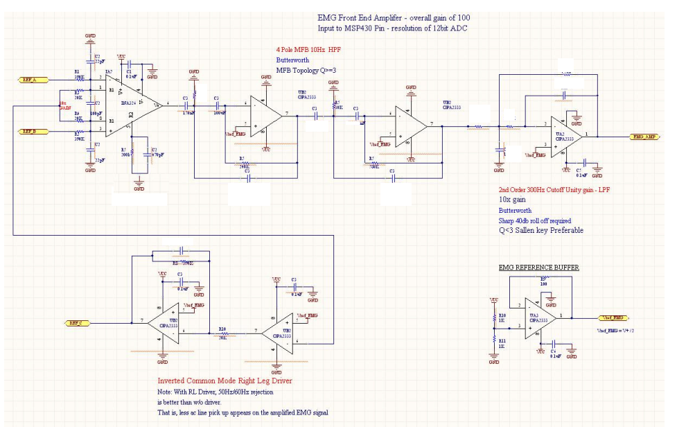
  1. The output signal of the INA326 is with an offset of almost -2.5V (I do not understand why but the diagram proposed by the manufacturer is being used)
  2. The output signal of the High Pass is mounted on 0
  3. Notch output signal is mounted on 0
  4. The Low Pass filter signal is mounted on 0
  5. The output signal of the Inverter Amplifier is set to -200mV voltage, which varies depending on the gain but reaches -1V (I do not understand why this happens the truth). In filters 2,3,4 and 5 the OPA4188.

The output of the adder is mounted, depending on the gain of the amplifier, between 1.5 and 2V instead of about 2.5 as it should be. Texas Instruments OPA188 is used
I do not know the offset to what the truth is ... I already reviewed the Datasheet and I do not find that part ... will it be the configuration?

The signal at the INA output has an approximate 500mV offset and a ~60mV peak-peak signal mounted on the offset and in Pasa Altas has an amplitude of ~60mV peak-peak (depends on the input) mounted on 0. After the Notch is mounted at ~ -40mV and the amplitude was decreased despite having unity gain. The output of the Low Pass is mounted on ~ 20mV and the amplitude decreases a bit more (can we attribute those losses to the tolerances of the components).

I also attach the images with the problem. 
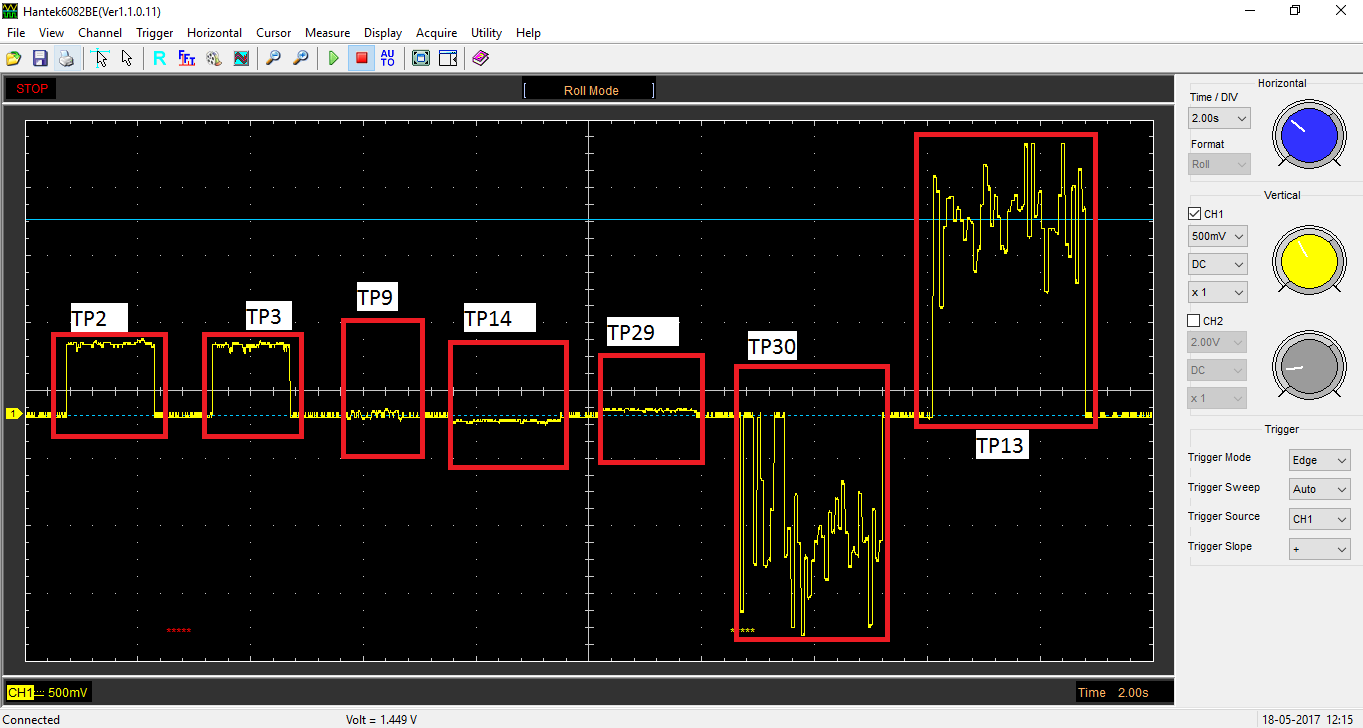
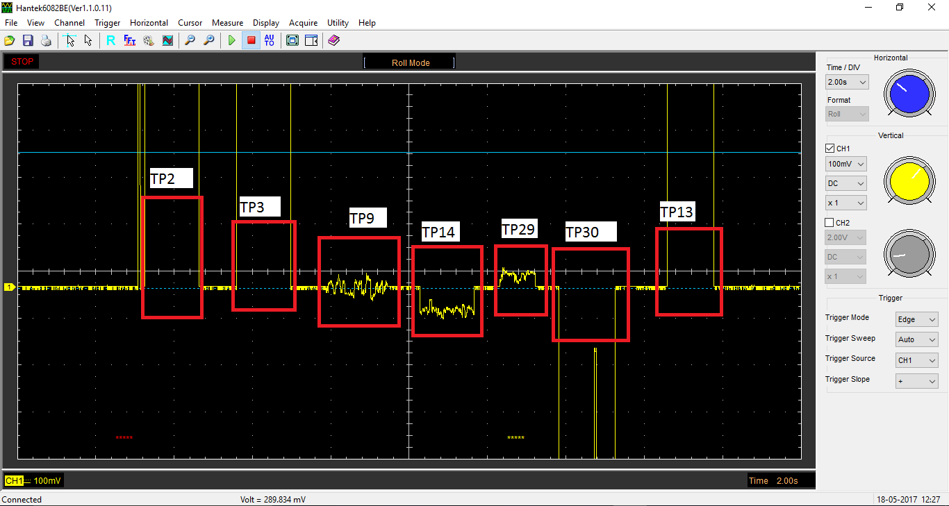
and a closer look:

Where do the offsets come from?

  • Hello Miguel,

    We have several questions.

    1. By "mounting" do you mean offseting?
    2. Is U8 your "adder" amplifier?
    3. What is the input signal and input circuity driving the INA to cause a -2.5V offset? Please clarify this situation.
    4. Additionally, what input signal are you driving the INA to cause the DC oscilliscope measurements you attached? How did you get all of the separate test points onto one plot?
    5. Does the ADC_REF2V5 pin come from an ADC that is internally buffered? Adding this offset at the non-inverting terminal of U8 loads TP30 down.
    6. Where is the ~60mV peak-peak mounting?

    Peter Iliya
    Precision Amplifiers
  • Peter Iliya said:
    By "mounting" do you mean offseting?

    Yes. Im offseting the signal 2.5V in order to eliminate negative voltages and use the whole signal since I need to use FFT later

    Peter Iliya said:
    2. Is U8 your "adder" amplifier?

    Yes it is

    Peter Iliya said:
    3. What is the input signal and input circuity driving the INA to cause a -2.5V offset? Please clarify this situation.

    Im using EMG signals. I don't have the reason for that... It changes since the last time I measure it today, the signal had a ~500mV offset. The circuit is powered with the TPS72325DBVT and the TPS79325DBVR. 

    Peter Iliya said:
    4. Additionally, what input signal are you driving the INA to cause the DC oscilliscope measurements you attached? How did you get all of the separate test points onto one plot?

    I literally amplified noise. I didn't connect anything to the input since the cable broke. But even with EMG signal this behavior is present. I just went from one TP to another fast enough to be able to show all of them. I set the time on 2sec division. 

    Peter Iliya said:
    5. Does the ADC_REF2V5 pin come from an ADC that is internally buffered? Adding this offset at the non-inverting terminal of U8 loads TP30 down.

    No. ADC_REF2V5 comes from a REF3125AIDBZT. I attach the image for you to see how is it connected:

    I did not understand "Adding this offset at the non-inverting terminal of U8 loads TP30 down" but the circuit is supposed to center the signal  at 2.5V so I can have a signal from 0 to 5V. The amplifier is supposed to amplify the signal from +/-mV to +/-2.5V. 

    Peter Iliya said:
    6. Where is the ~60mV peak-peak mounting?

    Thats the signal seen on TP9, which is correctly mounted on 0. 

    The signal should be mounted on 0 on the High Pass filter, the Notch, the Low Pass and the inverting amplifier until it is mounted on 2.5V on the last stage. 

  • Hey Miguel thanks for the answers.

    I ask about the INA326 input circuitry because if you do not have DC/return paths for you input bias current, then your inputs will begin to float or charge up. This will ultimately cause your output to fluctuate and eventually slam into one of the power rails. This may be why you keep measuring different offsets (e.g., 500mV, -2.5V) at the output of your INA326.

    You can find the explanation for this in most of our INA datasheets. See page 11 for the INA326 datasheet, but I’ll show a more comprehensive figure from the INA188 datasheet below as an example. Consider connecting shunt resistors to ground off each of your inputs. You can start with 47kOhm, but the best value will be based on your application.


    After you do this, then try driving a distinguishable signal into your INA to see how the circuit acts because inconsistencies in your current oscilloscope images may be noise related. What’s the potentiometer set to for U3 feedback resistance?

    Additionally, you want to be careful of the large 8.87M resistors R7 and R10. The input bias current of the OPA188 is specified to +/-160pA typically, which would create an offset of +/-mV on the input of U3.

    Overall you should be getting a 2.5V offset signal at TP13 since your 2.5V reference will be divided down to 1.25V at the Vin+ of U8 and then gained up by 2V/V back to 2.5V.

    Peter Iliya
    TI Precision Amplifiers

  • Hi Peter

    Let me see if I get it right.

    Peter Iliya said:
    I ask about the INA326 input circuitry because if you do not have DC/return paths for you input bias current, then your inputs will begin to float or charge up. This will ultimately cause your output to fluctuate and eventually slam into one of the power rails. This may be why you keep measuring different offsets (e.g., 500mV, -2.5V) at the output of your INA326.

    I need to connect both inputs to GND even when the body is connected to GND too?It is supposed that the EMG signal has a DC offset, because of the electrodes, which is normal, but if could be incrementing for what you just said. 

    Peter Iliya said:
    After you do this, then try driving a distinguishable signal into your INA to see how the circuit acts because inconsistencies in your current oscilloscope images may be noise related. What’s the potentiometer set to for U3 feedback resistance?

    The signal is noise. Im taking new images with EMG data but the problem is the same (I might be having some problems with the connector as well). I don't know the value of potentiometer at the amplifier but I do know that, yesterday, the signal moved from -200mV to -1V when moving the pot. Which corresponds to the signal being mounted on 1.5 instead of 2.5

    Peter Iliya said:
    Additionally, you want to be careful of the large 8.87M resistors R7 and R10. The input bias current of the OPA188 is specified to +/-160pA typically, which would create an offset of +/-mV on the input of U3.

    You mean I should use lower values there??

    Peter Iliya said:
    Overall you should be getting a 2.5V offset signal at TP13 since your 2.5V reference will be divided down to 1.25V at the Vin+ of U3 and then gained up by 2V/V back to 2.5V.

    Here I don't understand. You are saying that the 2.5V are being split in half but U3 in which stage? U3 is the OPA4188... and the U3 is not connected to the 2.5 offset signal... It is in the OPA188, in the adder.  I don't understand the last part. 

    thanks

  • Hi Peter

    I attach the images from the original signal. The EMG signal

    **Edit:

    What I don't get is why the NOTCH is adding such a big offset when the OPA4188 is supposed to have a max. offset of 25uV...

    Would It work if I add a capacitor in serie with the amplifier input for it to also work as an additional High Pass filter with amplification but with the signal output centered at 0 before the adding configuration to offset the signal 2.5V now for sure?? 

    Best regards

  • I saw a post: e2e.ti.com/.../2308.1-dsgn.bmp
    the image, the INA is the 326 (apparently) and they (we will only focus on the inputs) a resistor and a capacitor for decoupling. Would that work as the bias current DC path?? (There is a third electrode connecting the person to GND )
  • I’ll try to address your questions in order.

    - I’m not sure that if the patient/person is connected to ground that this will provide a path for the INA input bias current (Ib), but I assume not because this skin-interface impedance may be very high. Electrodes can have a DC offset, but this is not the reason why your floating inputs will cause the INA output pin to fluctuate.

    The image you included from a previous E2E post (http://e2e.ti.com/cfs-file/__key/CommunityServer.Discussions.Components.Files/14/2308.1-dsgn.bmp) shows 22pF capacitors (C2) connecting the INA326 inputs to ground, but these are NOT paths for the Ib current to flow through since these capacitors are open at DC. I’m not sure where the path is in the schematic, but in the same thread it is mentioned that these paths must be included as seen with this quote:

    “You must create a DC bias at the inputs (i.e. through pull up resistors to VREF) to ensure an IB return path and therefore, linear operation of the INA333.” – Matt Hann
    https://e2e.ti.com/support/amplifiers/precision_amplifiers/f/14/p/347/224360?tisearch=e2e-sitesearch&keymatch=emg#224360

    Overall, you have to connect some paths for the DC Ib going through inputs of the INA326, or else your output will be subject to an indefinite offset. Correcting this issue might correct other problems whether or not you’re measuring noise or EMG electrodes so I would start with this.

    - I think it would be best to determine the actual potentiometer resistance in order to know the gain and see if the U3 amp is behaving as expected and to know what offset if any there is at TP30

    - Resistors R7, R10, and R61 in your notch filter can be reduced (and capacitors increase to keep same fc) and this will reduce the offset seen by U3 because its Ib (150pA) won’t generate significant voltages across the resistors.

    - Lastly, I should correct myself. I meant to say that the 2.5V reference will be divided down to 1.25V at the Vin+ of U8, not U3 (I went back and corrected this.) Thus your signal at Vin+ of U8 is offset by 1.25V. This is then multiplied by 2 to give you a 2.5V mounted signal at TP13. TP30 should be centered at 0V.


    Peter Iliya
    TI Precision Amplifiers Tucson

  • Peter Iliya said:
    - I’m not sure that if the patient/person is connected to ground that this will provide a path for the INA input bias current (Ib), but I assume not because this skin-interface impedance may be very high. Electrodes can have a DC offset, but this is not the reason why your floating inputs will cause the INA output pin to fluctuate.

    Ok. I think I saw in a book that the capacitor from line to GND is use to isolate the patient and protect him/her from the transient voltages and so. But let me check again. I could use a resistor as on the example you sent me. The microphone one. Or is there any example for EMG signals? 

    Peter Iliya said:
    The image you included from a previous E2E post (http://e2e.ti.com/cfs-file/__key/CommunityServer.Discussions.Components.Files/14/2308.1-dsgn.bmp) shows 22pF capacitors (C2) connecting the INA326 inputs to ground, but these are NOT paths for the Ib current to flow through since these capacitors are open at DC. I’m not sure where the path is in the schematic, but in the same thread it is mentioned that these paths must be included as seen with this quote:

    I think the capacitors are for the patient to be protected. Ok, clear. Mmmm the path must be a resistor to the GND then right?

    Peter Iliya said:
    Overall, you have to connect some paths for the DC Ib going through inputs of the INA326, or else your output will be subject to an indefinite offset. Correcting this issue might correct other problems whether or not you’re measuring noise or EMG electrodes so I would start with this.

    Ok, understood. Ths way the offset will be always constant and not having any saturation problem right? (if the signal is not above the power voltage of course)

    Peter Iliya said:
    - I think it would be best to determine the actual potentiometer resistance in order to know the gain and see if the U3 amp is behaving as expected and to know what offset if any there is at TP30

    It is at 77K. 

    Peter Iliya said:
    - Resistors R7, R10, and R61 in your notch filter can be reduced (and capacitors increase to keep same fc) and this will reduce the offset seen by U3 because its Ib (150pA) won’t generate significant voltages across the resistors.

    Could this be causing the abnormal behavior of the circuit? At least that particular stage? That the resistors are too big the configuration is inverting the voltage and adding so much offset? What range of values would you recomend? 

    Peter Iliya said:
    - Lastly, I should correct myself. I meant to say that the 2.5V reference will be divided down to 1.25V at the Vin+ of U8, not U3 (I went back and corrected this.) Thus your signal at Vin+ of U8 is offset by 1.25V. This is then multiplied by 2 to give you a 2.5V mounted signal at TP13. TP30 should be centered at 0V

    So if the signal was correctly centered in 0V, the output signal would be at 2.5V as supposed no?

    Thanks!!

  • I don't think there are any EMG examples, but I think the microphone example may be best if your electrode is creating a differential voltage signal.

    Yes, adding these shunt resistors to ground will keep the offset constant.

    The large offset cause by the U3 Ib and large notch resistors will be an offset that is carried throughout your signal chain and affects DC level accuracy and possibly AC. This ~2mV offset at TP14 may be the reason your TP30 measurements are not mounted at 0V. This DC offset is gained up at U3 making your offset from 0 even worse.TP13 measurements look correctly offset at 2.5V.

    I recommend reducing the R7 and R10 (maybe R61) to reduce your offset cause by Ib of U3 and fixing you INA input circuity by adding DC resistive paths to ground.
  • Peter Iliya said:
    I don't think there are any EMG examples, but I think the microphone example may be best if your electrode is creating a differential voltage signal.

    yeah... I was looking for some examples and there were none... not even on Google... I found some similar circuits but with the right leg circuit for ECG and some other for EMG but without the resistors. 

    How can I calculate a good resistor value for the EMG signal? it goes from 1.5 to 15mV

    Peter Iliya said:
    Yes, adding these shunt resistors to ground will keep the offset constant.

    Perfect. That way the offset will be always the same, the INA wont be saturated and will always work properly right?

    Peter Iliya said:
    The large offset cause by the U3 Ib and large notch resistors will be an offset that is carried throughout your signal chain and affects DC level accuracy and possibly AC. This ~2mV offset at TP14 may be the reason your TP30 measurements are not mounted at 0V. This DC offset is gained up at U3 making your offset from 0 even worse.TP13 measurements look correctly offset at 2.5V.

    The offset on the INA is solved thanks to the High pass filter. The offset at TP14 is about 40mV. and after the Low Pass (TP29) the offset is around 20mV. 

    Peter Iliya said:
    I recommend reducing the R7 and R10 (maybe R61) to reduce your offset cause by Ib of U3 and fixing you INA input circuity by adding DC resistive paths to ground.

    I will. I will look for a lower resistors, in K instead on M. And I will connect the circuit in a breadboard just to check the offsets... Because the actual circuit is mounted already on a PCB with the MCU Im using... 

    So, adding the paths to GND at the inputs will make the offset stable. I also need to add some capacitors there for patient protection (Is that ok if I add the capacitors (as on the link I provided) in parallel to the resistors? )

    Then change the resistors and the capacitors on the Notch

    And just to be sure to have the offset at 0V before the amplification, I could add an additional capacitor in series with the input of the amplifier, change the POT to R23 and set a big fixed resistor at R18 (R19 disappears) to be able to modify the gain without changing the cut-off frequency of the additional High pass right?

    THanks!

  • Hello again,


    When choosing these resistor values you have to compromise because you don’t want them to be too small and drain too much current from your signal, but you don’t want them to be too big and add thermal noise. I can’t recommend a specific value because I am not familiar with your system, but you may want to experiment with this in your prototypes.


    Adding the shunt resistors does not mean your Vos offset of the INA will be constant. This can vary with the frequency and common mode of the signal from the EMG. Your INA could also saturate if the amplitude of the EMG sensors is too high. You will need to consider what the possible amplitude range of your sensor is when implementing the gain of the INA.


    Adding capacitors to ground in parallel with these shunt resistors should be fine.

    Miguel Amezcua Peregrina said:

    And just to be sure to have the offset at 0V before the amplification, I could add an additional capacitor in series with the input of the amplifier, change the POT to R23 and set a big fixed resistor at R18 (R19 disappears) to be able to modify the gain without changing the cut-off frequency of the additional High pass right?


    I am not sure which amplifiers you are referring to, but if you add an in-series capacitor where TP29 then you effectively remove the offset before amplifying the signal just make sure the capacitor’s equivalent resistance is at least a decade lower than R23 to reduce gain error at U3.


    You would also be able to adjust this gain if the potentiometer is moved to R23, yes.


    Best,

    Peter Iliya

    Precision Amplifiers

    Tucson, AZ

  • Hi Peter

    Peter Iliya said:
    Overall you should be getting a 2.5V offset signal at TP13 since your 2.5V reference will be divided down to 1.25V at the Vin+ of U8 and then gained up by 2V/V back to 2.5V.

    I have a question n this part. This gained would also modify the amplitude of the original signal no?

  • If signal directly feeding into U8 IN+ is 2.5mV peak-peak and centered around 1.25V, then TP13 will read 5mV peak-peak centered around 2.5V. So the answer to your question is yes.