This thread has been locked.

If you have a related question, please click the "Ask a related question" button in the top right corner. The newly created question will be automatically linked to this question.

INA126: Error in gain calculation ?

Part Number: INA126

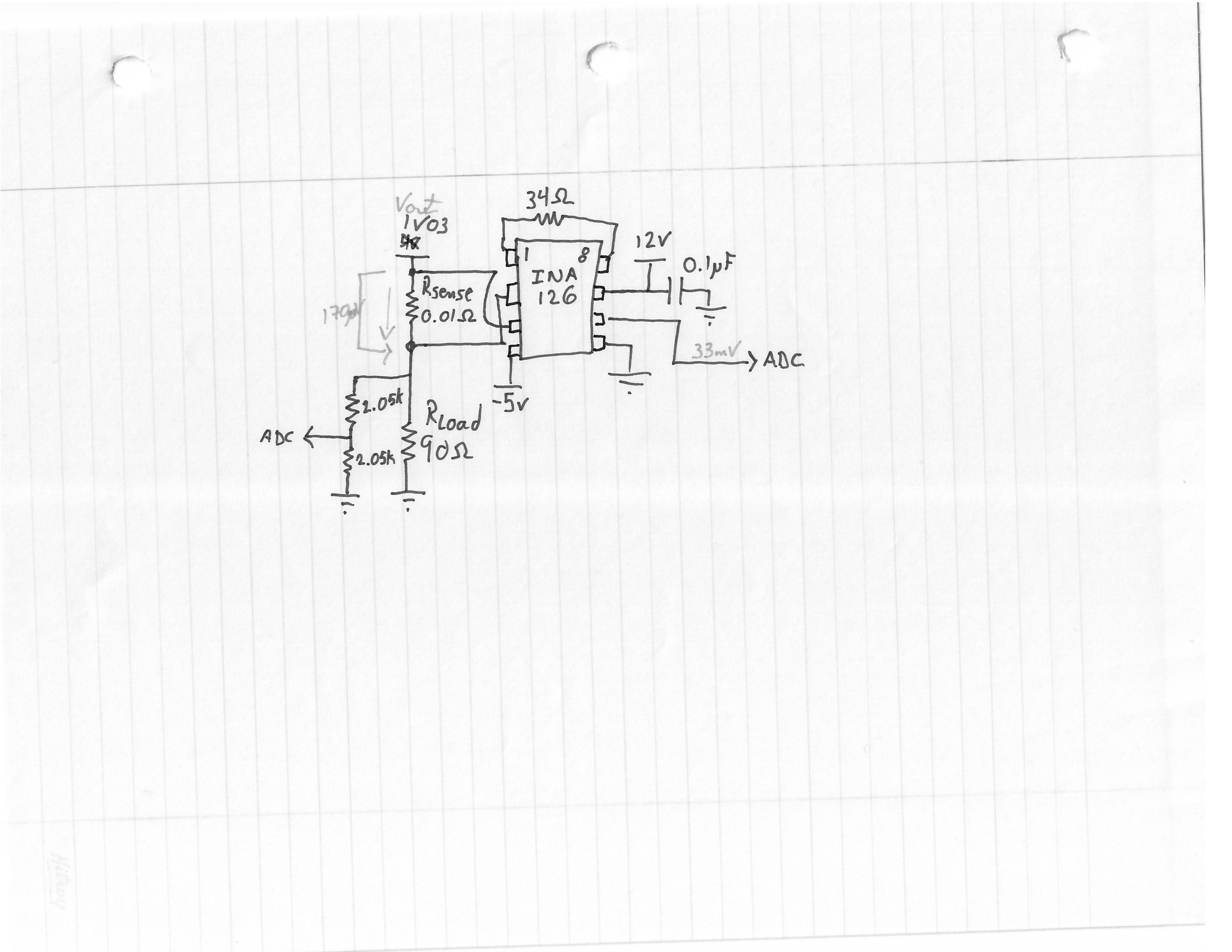
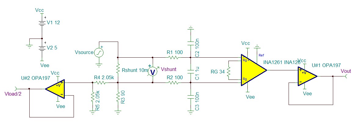
I uses the INA126 to amplify a high side current sense resistor (0.01ohm).

In my test the Vload is 1.03V

The load is 90ohm

the V(rsense) is 170uV

the gain resistance RG is 34ohm -> gain = 2357

The INA126 output is 33mV -> Gain of ~200

I know the numbers does not add's up. I have some noise and my equipement is not suitable to measure below mV voltage.

Also, if Vout is 0, the INA126 output is below 0.

The INA connects directly to the resistor pads using kelvin connection.

The ina126 is powered with +12V, -5V and the REF pin is connected to GND (as it can be seen on the diagram).

I don't understand what is going on.

Do you have any idea of what is going on and why the gain is so wrong ?

Thank you a lot

  • Hello Christian,

    Your RG value is correct based off the equation in the datasheet. I will run some circuit simulations and let you know if I find any issues.

    Best regards,

    Errol Leon
    Texas Instruments
    Precision Amplifier Applications Engineer
  • Hi Christian,

    I have a few concerns with this design:

    1) The first is the ADC on the input side to read the load voltage. Though it depends on the ADC, I do not believe you will get a very accurate reading using the configuration as shown. A better method would be to buffer the load voltage with an amplifier to drive the ADC with a low impedance.

    2) My second concern is how you have determined the voltage drop across the shunt resistor. It is not possible that with a 1.03V source you would see a 170uV drop across the shunt resistor with a 90 Ohm load. The reason I say this is because this would imply a current through the shunt resistor of 17mA. This current flowing through the load resistor would result in a voltage of 1.53V, higher than your supply voltage! This would imply current was actually flowing into your supply from the load.

    3) Lastly, with the reading you are seeing I am led to believe that you are measuring the output voltage using the ADC. However, with the INA126 in such a high gain configuration I can confidently say that with just about any converter you will not be able to get an accurate reading from the ADC. If you are using something like an 8-bit converter with a very long acquisition time, then you may be able to get away with it, but otherwise you will need more bandwidth driving the ADC. To address this, you would again want to add a buffer amplifier with sufficient bandwidth and a properly selected output filter to obtain accurate results. As a quick test I would suggest disconnecting the ADC and measuring the output of the INA126 with a multi-meter. I would double check the input as well to be sure you are seeing the correct value.

    If the voltage you are seeing is not read from the ADC and you have verified that the input signal is at the proper level, then the issue may lie elsewhere. Flux contamination is another common issue that can result in invalid readings so you may also want to make sure you have properly cleaned your board and eliminated any excess flux, as this can result in parasitic paths that cause current to flow in places it has no business being!
  • Thank you Zak and Errol,  I appreciate your answers.

    To reply your comment zak,  

    1&3. Thank you for your point. I did not see that during the design phase. So, I will try to use a standard 3 opamp instrumentation opamp.

    2. I agree with you that there is a problem with the measurements and I cannot understand where is the problem. I think the problem can come from my dmm, it is not precise enough for uV measurements or maybe it is because of the fact : The voltage 1.03V is from a buck regulator (1.5MHz). The voltage ripple is 2mV with spike to 30mV with some LC ringing at the pwm frequency. But, since the opamp is differential, I would have thought the noise would be eliminated. The image show the signal to gnd on the Rsense. I take my measurements in AC mode to remove the DC offset.

    Thank you

  • Christian,

    A standard 3 op-amp INA will tend to offer better performance for both common-mode rejection and ADC drive since the bandwidth of the output stage is independent of the gain. However, these still tend to be low bandwidth devices and depending on what you are attempting to drive and the speed of the converter, you may still need a buffer between the converter and the INA. The CMRR of the INA will cut down the amplitude of the oscillation on the output, but for better performance I would suggest including a filter on the input. I have attached an example TINA file showing these changes.

     INA126 Output Error.TSC

  • Thank you a lot Zak,

    I will modify my design with your suggestion. Thank you a lot for your help!