This thread has been locked.

If you have a related question, please click the "Ask a related question" button in the top right corner. The newly created question will be automatically linked to this question.

XTR108: the output voltage of the XTR108 cannot change.

Part Number: XTR108

Hello
I have a problem with XTR108, my circuit is according to datasheet XTR108 and XTR108 EVM/ FIGURE 1. RTD(PT1000) Input, voltage  Excitation,input resistant is adjusted in range 900Ω - 1100Ω.Expected voltage  is 1V~5V, XTR108 output is 0.5V~2.5V.
1.  When i debugging  the circuit, the output voltage is 0.895V, and cannot change. And the current of pin1(VI-0) , pin2(VI-1) is 0mA. the voltage of pin1  pin2  is zero.

2. I want to known  the Parameter requirements of diode in the charge pump circuit. Can I replace it with two diode(1N4148)?

Thanks for help

  • Hi user5222239, 

    1. Would it be possible to get a more complete schematic with resistor values? Also, the register contents (or EEPROM contents) of the XTR108 would help with troubleshooting. With this information, we can derive what the expected output behavior of the XTR should be. 

    2. I don't believe there is a required specification for the charge pump diodes. The XTR108 datasheet suggests a BAV99 diode, which appears to be a small-signal silicon diode - a 1N4148 should work in this application as well.

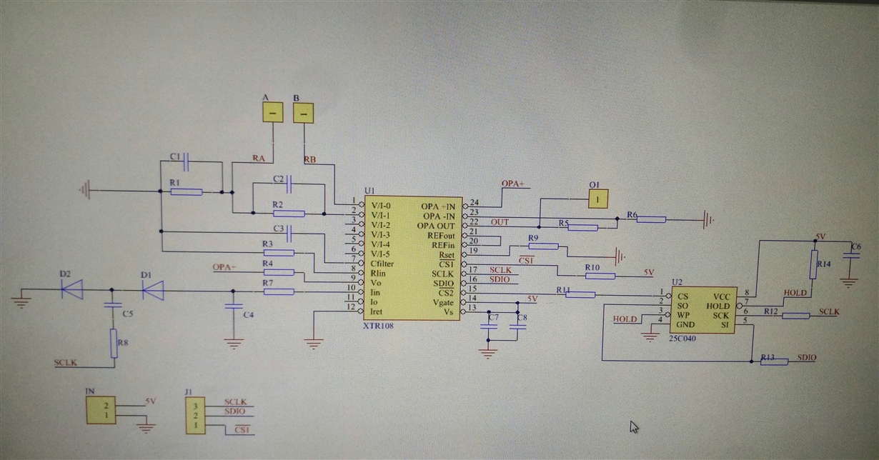
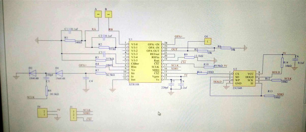
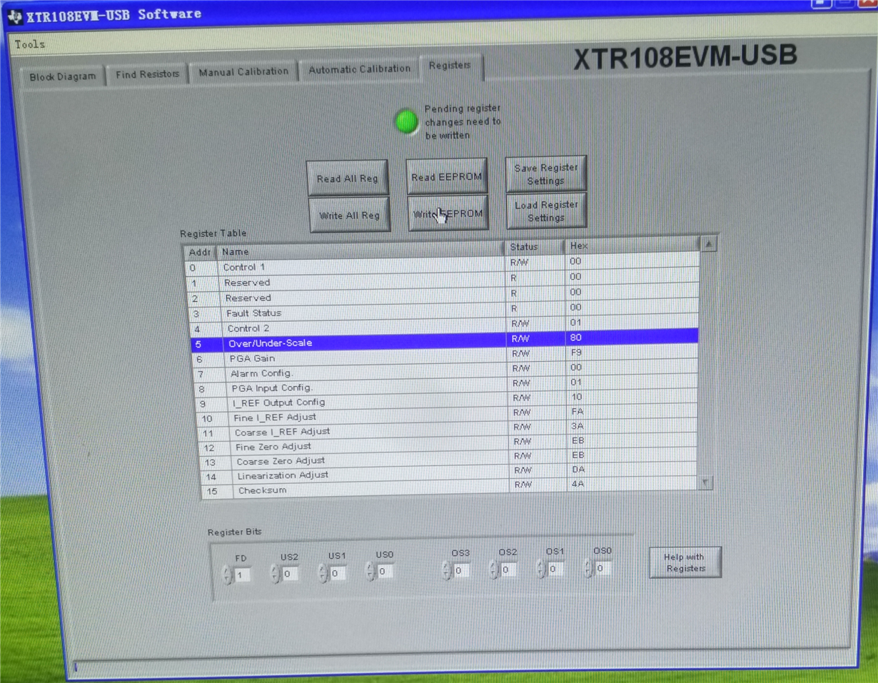
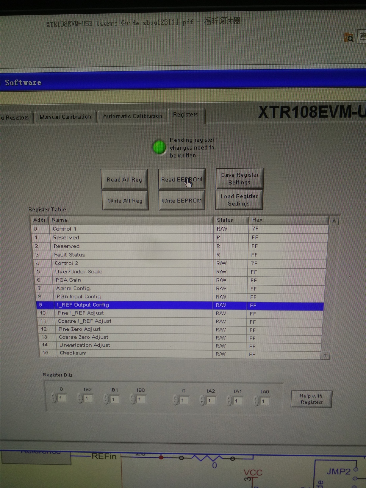
  • The problem appears in the debugging process,I donnot  change the register contents (or EEPROM contents) of the XTR108.  The value of the schematic is shown in fig1.

    When I debugging the XTR108 EVM circuit , I foud that the" XTR108EVM-USB Sensor Board" is not the  same as the schematic in the “user`s guide”(XTR108EVM-USB Evaluation Board and Software Tutorial). In the "XTR108EVM-USB Sensor Board" the signal "SPI_SCK" is not connecting with the "charge pump circuit",and the output voltage is also right, Is that right?  Please help me with this question, Whether you have a new version “user`s guide”?

    And when I disconnect "SPI_SCK" is not connecting with the "charge pump circuit", the output voltage of the circuit become to 0mV.and cannot change with input resistant(PT1000). And the current of pin1(VI-0) , pin2(VI-1) is 0mA. Please help me with that  problem?

    Is  the current onpin1(VI-0) , pin2(VI-1)  continuous after the chip is powered? And in what case the current will disappear?

    Thanks for your help!

  • Hi user5222239,
    The version of the XTR108EVM users's guide available from the product page should be the most recent. Looking at the design files, I see no differences between the sensor board schematic in the user's guide and the latest version we have locally. The EVM does have the option of disconnecting that charge pump in order to user the XTR108 in current-output mode.

    Regarding debugging the output issue, it's very important to know the register/EEPROM values, since they control routing of the excitation current, PGA inputs, and excitation routing. Without knowing this information, it's going to be very difficult to debug this issue.
  • Thanks for your quick reply!AND I debugged the "XTR108 EVM Board" and my own circuit again. my goal is use voltage mode with 0V~2.5V output,And I still have some problems with XTR108.

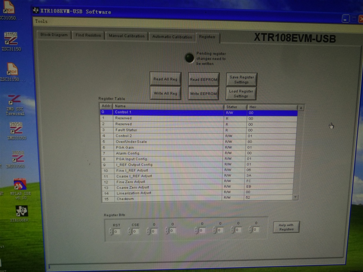
    1.    For "XTR108 EVM Board":   the register is shown in fig1.The current of pin1(VI-0) and pin2(VI-1) is existence, but the ouput voltage is 0V, and the output voltage don't change with the input  resistant(PT1000).   Why?  BUT  last week I debugged the "XTR108 EVM Board" according to the user guide,the output voltage is right.    Please help me with the question, thank you! 

    The detailed circuit settings shown below:

    a) the jumper is :  JMP1: Bypass FET;   JMP2: Bypass FET;  JMP3: Voltage Mode;  JMP4: No Load (Voltage Mode);  JMP5: Use Charge Pump;  

                                    JMP6: Bypass Buffer;  JMP7: Charge Pump CLK = SPI_SCK;  JMP8:2-Wire RTD.                           

    b) The Power supply voltage is 5.1V.                               

    c) The resistants of  Rz  Rlin   Rcm   Rset  is set by the debugging sofware,                   

    d) The temperature is set from -10℃~60℃.  

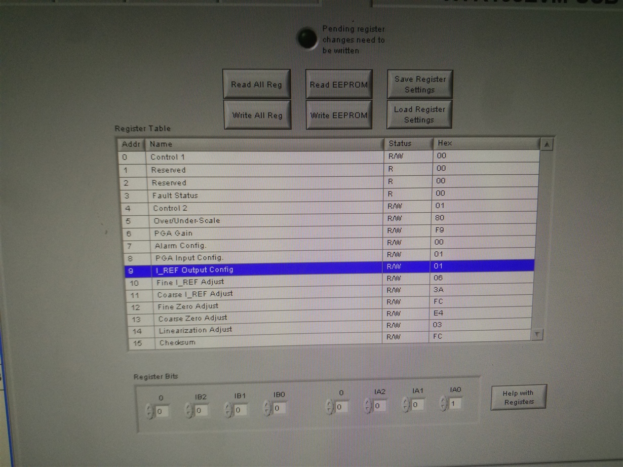
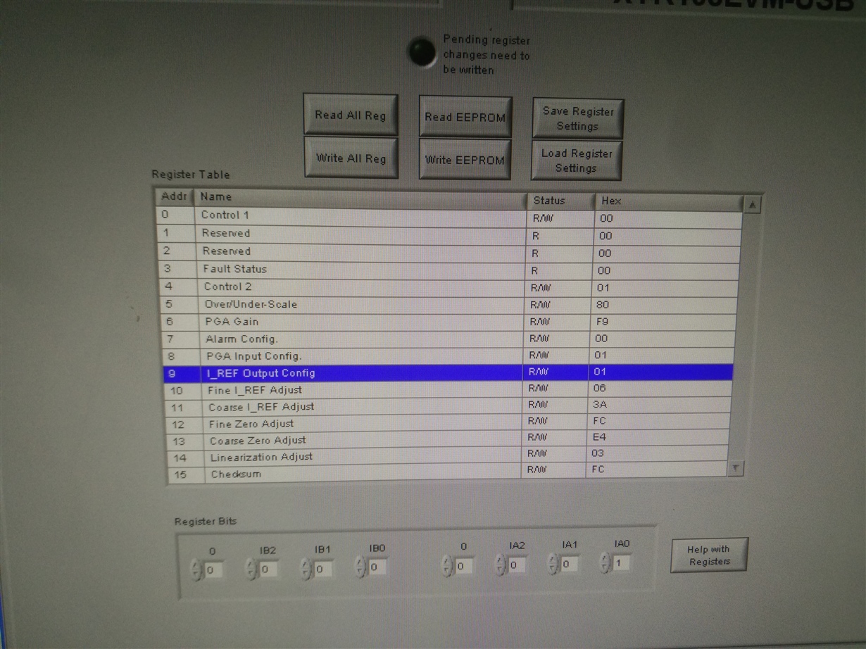
    2   For my own circuit, the register is shown in fig2. I have changed the I_REF Output config from ff to 01, After I changed the register the current of pin1(VI-0) and pin2(VI-1) is existence ,BUT the output voltage is still 0V.why? Please help me with the question,thank you!

    3.the circuit schematic is shown in fig3, I refer to the manual circuit, is there some problems in my circuit?

    4. When I debug the circuit, should I change the registera? If I need to change the registers, how to change it ? Do you have latest operation guide?

    5. Could you send me the source code of the " USB DAQ Platform", thank you!

                                                                                                                         fig1  the  register of "XTR108 EVM Board"

                                                                                                                          fig2      the register of my own circuit

                                                                                                                    fig3       the schematic of my own circuit

  • after debugging the circuit, i found the resistant of the interface board is not correct. so the ouput voltage can change with the input resistant(PT1000). but now the resistants can not keep stable and the output voltage can not keep stable with a constant input resisstant. one condition of the resiatant is shown below.
  • Hi user5222239,
    What do you mean by "the resistants can not keep stable"? Are the resistor values on the board shifting? How is this being measured?

    Source code for the USB DAQ firmware is not available. The source code for the XTR108 EVM can be found here: www.ti.com/.../sboc422
  • sorry I use the wrong word.  What  I mean  is  the registers of the XTR108 always change, as shown in fig1.

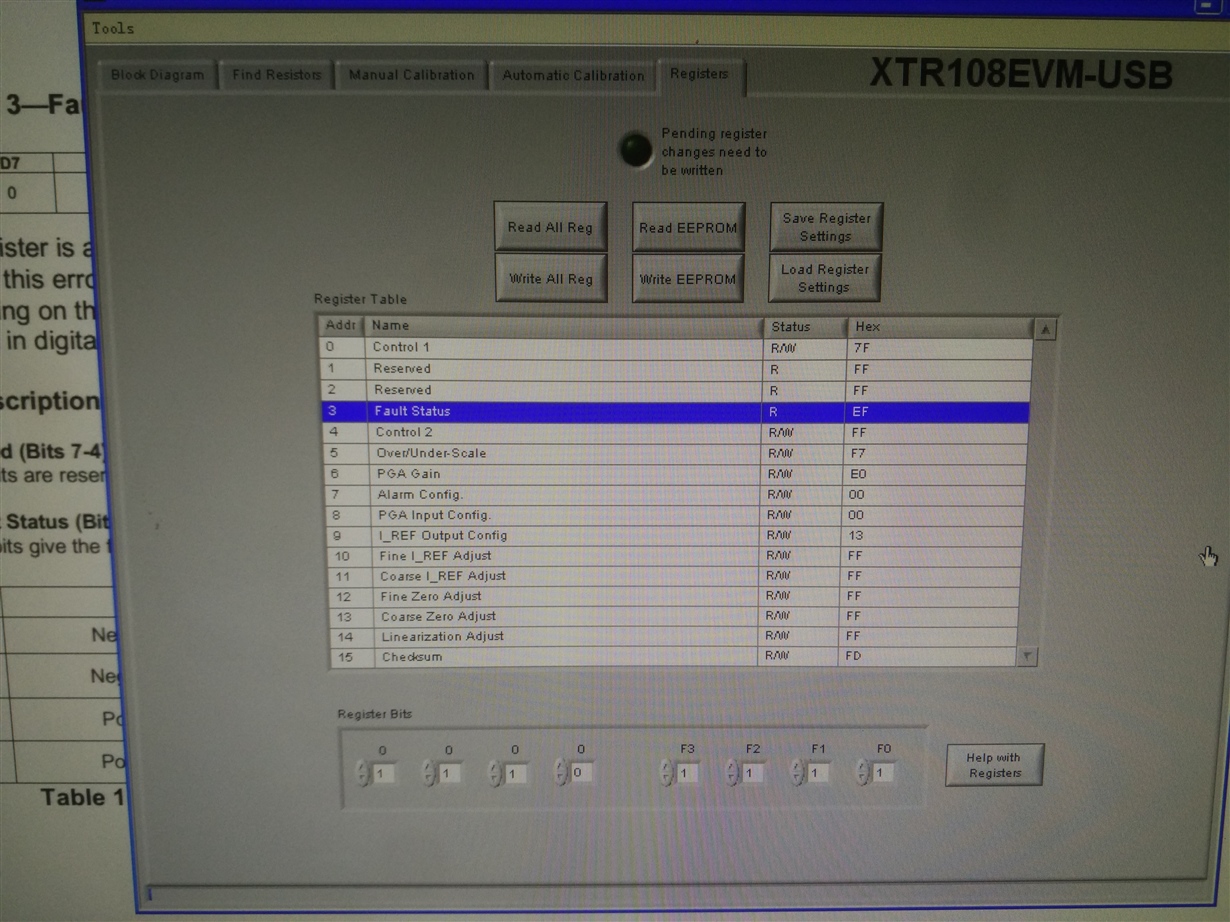
    After welding circuit board and give the circuit power the registers data is shown in  fig1. And I debug the circuit according to the Handbook“XTR108EVM-USB Evalua board and software tutorial”,the registers data can not turn to correct value as shown in fig2.  So  I change the registers  to the correct value as shown in fig2 with the Debug software,but when I clik the “calculate initial settings”button or the “read all registers”button,the registers turn into random data like fig1. I cannot debug the XTR108.  After that I tried several times to change the registers,the situation is same as before.

    Can  you  help me with the problem ,thanks very much!

                                                                                                                                              fig1

                                                                                                                                     fig 2

                                                                                                                    fig3   circuit schematic

  • Hello   Alexander, about my circuit i debug it again today, there are still some problems. This time I detect the signal of  the "CS2" and "SCLK" in the XTR108 through Oscilloscope.

    In the circuit of XTR108 EVM:

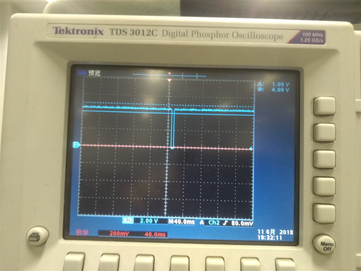
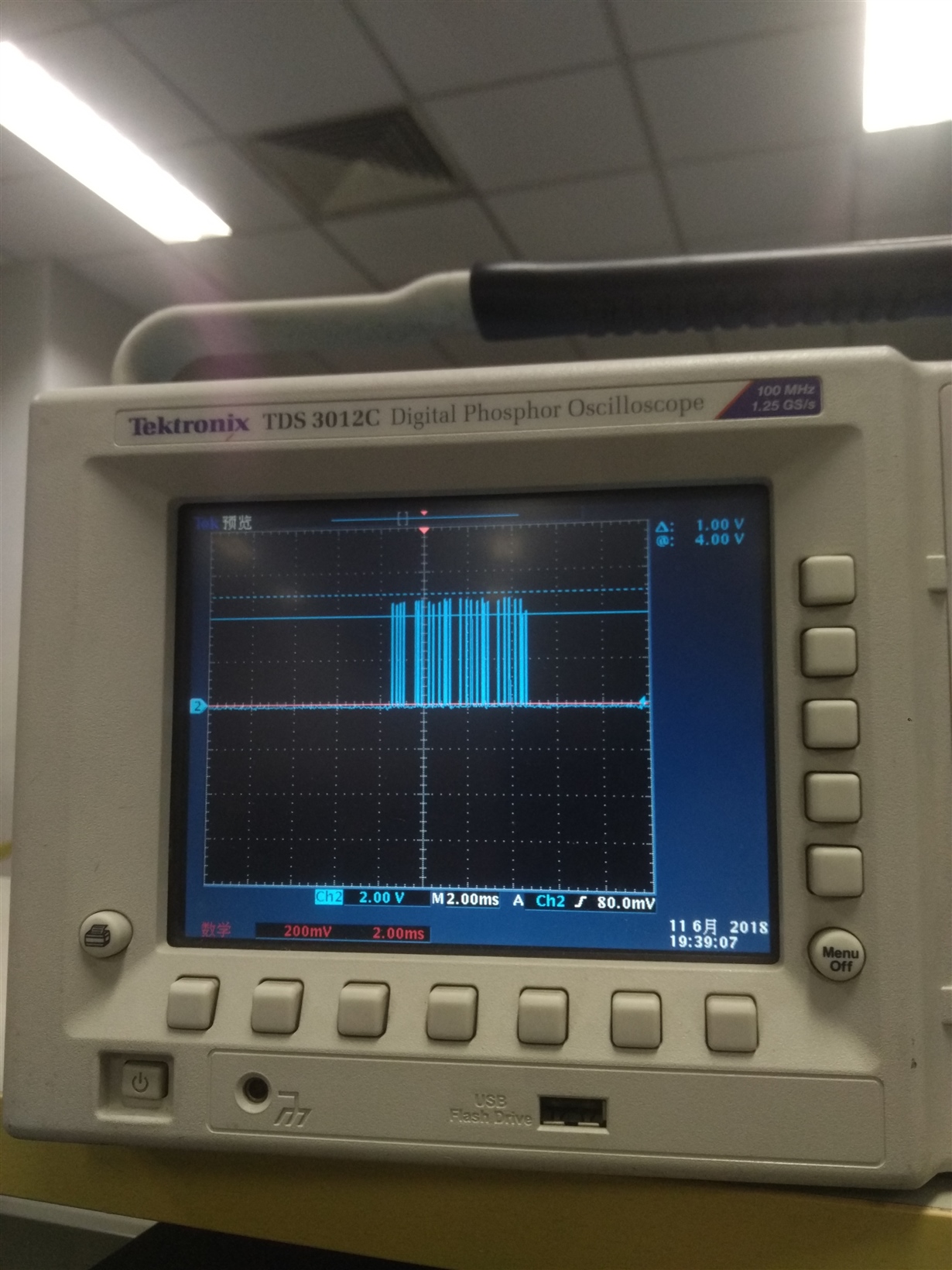
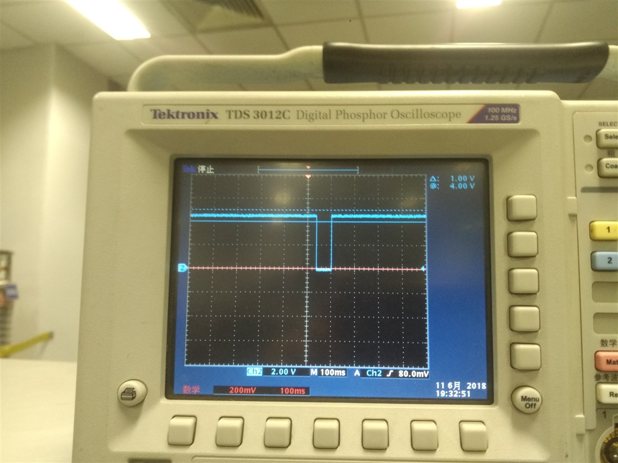
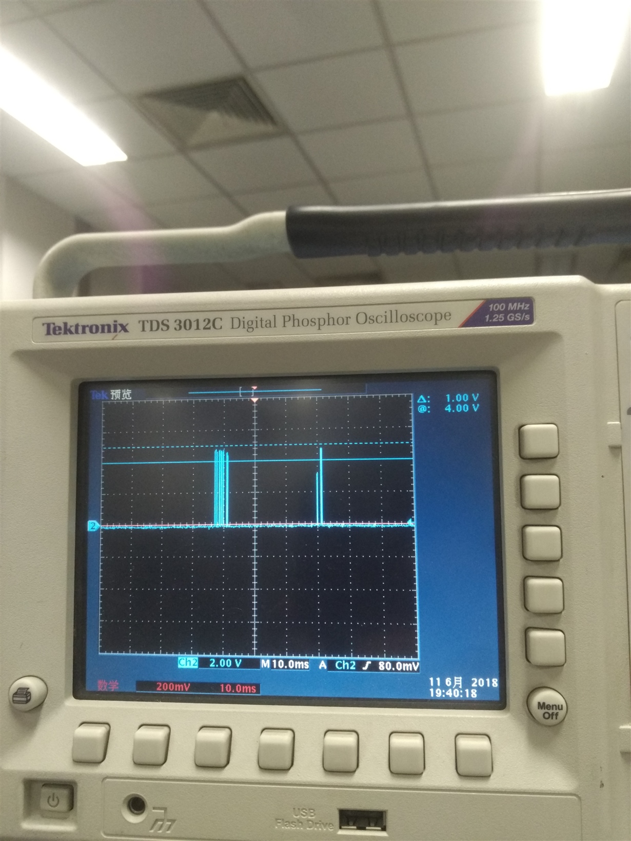
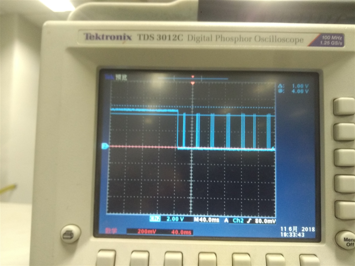
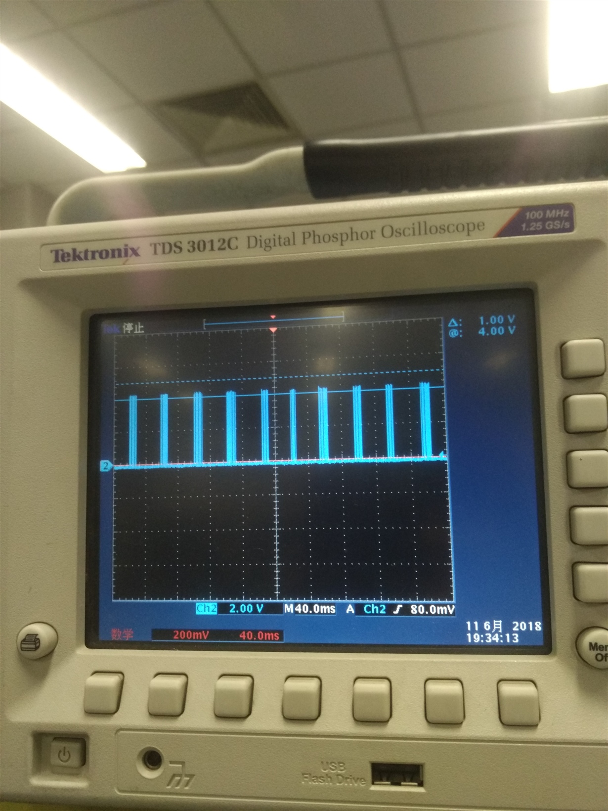
    1.when I click the "Read EEPROM"button,the "CS2"pin output a Low pulse, and "SCLK" output a few low pulse, the signal is shown in fig1  and fig2. and the registers is shown in fig3.

                                                                                               fig1

    fig2

    fig3

    2.when I click the "Write EEPROM"button,the "CS2"pin output a Low pulse, and "SCLK" output a few low pulse, the signal is shown in fig4  and fig5. and the registers can write to the EEPROM.

    fig4

    fig5

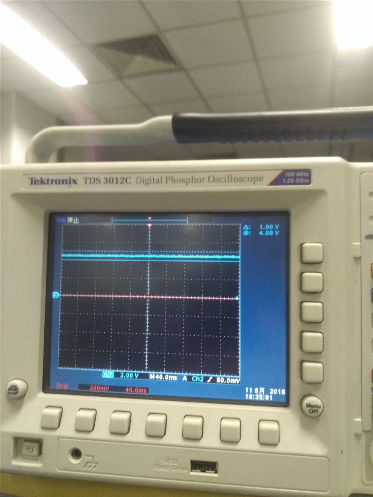
    3.when I click the "Write All Reg"button,the "CS2"pin and "SCLK" pin output high level voltage without low pulse. as shown in fig6.

    fig6

    4.when I click the "load Registers settings"button and then click the "Write All Reg"button,the "CS"pin and "SCLK" pin output high level voltage without low pulse. as shown in fig6.

    In my circuit which cannot work probably:

    1.when I click the "Read EEPROM"button,the "CS2"pin output a Low pulse, and "SCLK" output a few low pulse, the signal is shown in fig1  and fig2. and the registers is shown in fig7.

    fig7

    2.when I click the "Write EEPROM"button,the "CS2"pin output a Low pulse, and "SCLK" output a few low pulse, the signal is shown in fig4  and fig5. but  the registers cannot write to the EEPROM.

    3.when I click the "Write All Reg"button,the "CS2"pin and "SCLK" pin output high level voltage without low pulse. as shown in fig6.

    4.when I click the "load Registers settings"button and then click the "Write All Reg"button,the "CS"pin and "SCLK" pin output  continuous low pulse. as shown in fig14 and fig15.

    fig14

    fig15

    It is known by comparison that the difference between  two circuits are the "CS2" and "SCLK" when I click the "load Registers settings"button and then click the "Write All Reg"button,

    Can you help me analysis Why  my circuit will appear the situation described above.  Thank you !!!

  • Hi user5222239,

    It's difficult to say what could cause this difference. Some of the difference between the scope shots could just be due to the sampling rate of the oscilloscope, especially on a longer timebase, as above. If you have access to a protocol analyzer (even a basic one, such as a Bus Pirate or other microcontroller) that we could use to look at the raw SPI data, this would give us more information to work with. 

  • user5222239

    We haven't heard back from you so we assume you were able to resolve your issue. If not, post another reply below.

    Thanks
    Dennis