This thread has been locked.

If you have a related question, please click the "Ask a related question" button in the top right corner. The newly created question will be automatically linked to this question.

XTR115: Pin3 to Pin4 Resistance value Tolerances.

Part Number: XTR115

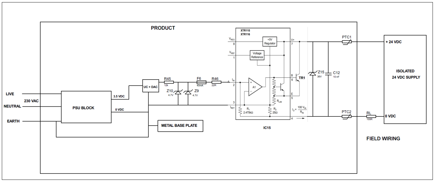
I am analysing failure modes on a product (4-20mA application) that use the XTR115.

I have measured about 26-30 ohms between pin 3 and pin 4 of XTR115.

However in modules that have failed, I have noticed the measurement to have changed (to anything from 0 to mega-ohms).

Please advise: What is the tolerance for the value, in the datasheet it is shown as 25ohms.

Please advise: What could cause this value to drift up or down.

  • Hi Victor,

    We do not characterize the tolerance of this resistor as it is not the value of this resistor that is important for the design, but maintaining the proper ratio between R1 and R2. You may see a shift in this value of +/-20%, but the ratio will be very accurate. If you are seeing excessive deviation in this parameter, then there are two possibilities: Either the board has not been cleaned and there are parasitic paths created by flux residue that are altering the measured value, or you have damaged the device with EOS. If you describe the failure conditions in more detail then I may be able to help you track down the cause.
  • Thanks for your response. 

    Here I further elaborate on the problems we are experiencing.

    Failure mode: The unit(s) randomly stop generating the (4-20mA) loop current.

    In our returned products lab, we have elected to measure the resistance value between pin3 and pin4 in order to determine the health status of the XTR115. It is a parameter that can be accessed while the component is in circuit.

    Our findings so far show the resistance to change( 0 ohms to Mega ohms). The change can be permanent or momentary.

    In cases where the change is permanent:- The loop current becomes disproportionate to input or disabled.

    In cases where the change is momentary:-

    After a series of testing (power-cycling), the measured value returns and stabilizes at 31ohms. 

    These units have been returned for dropping out (No loop current, while everything else is on).

    In our tests as manufacturer, the units are giving correct loop current.

    In your response, please include advice on  the following.

    • Can we rely on measuring the Pin3 and Pin4 resistance to determine the health state of the XTR115. 
    • Is the resistance quoted for  Pin3 and Pin4 coming from a passive or active component.
    • What could cause the XTR115 to momentary stop producing loop current. The stop can be a few hours. And at times the unit has to be power-cycled to re-establish the loop current.
  • Hi Victor,

    How are you measuring the resistance between pins 3 and 4? Is it directly at the pins or through external test points? I am wondering if something might be wrong at the pcb level or if this could be due to bad solder joints. The resistance between pins 3 and 4 is indeed a passive resistance and should not deviate that heavily. Can you verify that there is good connectivity between the pins of the XTR and the traces on your board?

    The momentary case is much stranger. If your loop supply dips heavily then the loop may be out of compliance for the XTR. Are you using an external transistor or relying on the internal transistor? If you use the internal transistor or an external transistor placed too close to the XTR then this could be a thermal issue. Understanding the conditions in which this occurs can help eliminate this as a variable. Does this typically manifest at higher output current levels?

    Another thing to consider is the kind of environment these are operating in and whether you have any transient protection in the loop. If the devices encounter an excessive overvoltage then this could result in damage that would tend to manifest as a fail open.

    I'm also not entirely convinced that this is not a board contamination issue. Have you tried cleaning the boards that exhibit the failure? The optimum cleaning depends on the kind of flux you use, and especially whether it is water soluble. We generally place our boards in an ultrasonic cleaner and then bake them in an oven around 75C to remove any flux residue. Hand cleaning has not always resolved the issue because the flux can end up trapped under components.

    You could also try swapping a failing unit onto a good board to see if the problem tracks the component or the board. Right now there are many variables that need to be eliminated before we can say for sure what the problem may be.
  • Hi Victor,

    if you look carefully at figure 1 of datasheet, you will notice that R2 connects the input and output side of XTR115. In an overvoltage condition R2 could provide a path for a surge current or an ESD event. This can occur if the input side has an unwanted connection to any potential from the outer world, like pretection earth or similar. Even capacitive stray coupling to the input signal from an enclosure sitting on an unsane potential can make R2 conducting too much current and becoming damaged. So, be careful when wiring the input circuitry of XTR115. If you have an enclosure for the XTR115 circuitry and you want to ground it, better connect it to pin 4 rather to pin 3.

    Kai
  • Thank you Kai and Zak.

    We are setting up a series of tests that take into your valuable advice. I will update you with our findings.

    In the meantime,..

    Please advise the expected time to failure of the XTR115 when it is run in the following mode

    • Continuously ON, 24hours a day, 365days a year.
    • loop current averaging 9mA.
    • Ambient temperature 60 to 85 Degrees Celsius.

  • Hi Victor,

    the increase in failure rate due to higher die temperature can be estimated by the help of Arrhenius equation. The acceleration factor AF, by which the failure rate increases is:

    AF = exp (Ea/k x (1/Tu - 1/Ts))

    In this link you can find the failure rate data of XTR115:

    www.ti.com/.../estimator.tsp

    As the majority of loop current is shunted through the external transistor and only a small portion of loop current is running inside the XTR115, the power dissipation within the XTR115 is minimal. It can be assumed that the junction is not heating up much above the ambient temperature.

    Assuming an activation energy of Ea = 0.7eV and taking k = 8.63 x 10^-5eV/K, Tu = 273K + 55K = 328K, Ts = 273K + 85K = 358K yields an acceleration factor of AF = 7.94. So, the failure rate will increase by a factor of about 8, when the die temperature is 85°C instead of 55°C.

    Wafer tests have shown a mean time between failure (MTBF) of 4,710,000,000 hours (60% confidence level). Taking into account the acceleration factor of 8 translates this to a MTBF of 588,750,000 hours at 85°C die temperature. So, at 85°C die temperature the MTBF is about 67200 years.

    Kai
  • Thank you for this advice.

    We indeed have functional earth connected to Pin3. Our Engineering team is going to avail me some schematics to share with you. 

    May I highlight to you that failures are being reported after 12months of product being in service.

    There are some further points that we need to clarified:

    From  

    …..maintaining the proper ratio between R1 and R2. You may see a shift in this value of +/-20%, but the ratio will be very accurate.

    • Question. What is the target value for this ratio? We have taken measurements from a brand new XTR115, R2=29.3ohms, R1=2708ohms. R1/R2=92.3. What values should we expect when read from our PCB? This can help us detect faulty soldering.

    …..The momentary case is much stranger. If your loop supply dips heavily then the loop may be out of compliance for the XTR. Are you using an external transistor or relying on the internal transistor? If you use the internal transistor or an external transistor placed too close to the XTR then this could be a thermal issue. Understanding the conditions in which this occurs can help eliminate this as a variable. Does this typically manifest at higher output current levels?

    • Please Elaborate on the term "Thermal Issue". At what thermal point is the product affected and to what effect?
    • In our design, an external Transistor (MJD47TH from ON Semiconductors) is employed. The emitter (of the Transistor) is approximately 7mm away from the XTR115. Is this distance adequate?.
    • The module is then potted with epoxy. Does this contribute to the thermal issue?

  • Hi Victor,

    you need functional earth being connected to pin 3? Oops!!! Not good!! This is the cause for the failures! If possible, connect functional earth to pin 4 and not to pin 3. If not possible, change the circuit! Connecting functional earth to pin 3 will damage the chip again and again!!

    Kai

  • Hi Victor,

    The resistors are scaled to provide a current gain of 100, so R1 is ~99x R2 and barring any measurement error you should see something close to this. For the thermal issue it's more of a concern if you are relying on the internal transistor, but it can still be a problem with an external transistor if the heat produced by Q1 changes the ambient temperature of the XTR by a significant amount. If the junction temperature exceeds 165C then the part will sustain damage. However, I do not believe you should see junction temperatures anywhere near this in your application unless the ambient is already very high. The epoxy may have a slight impact on this because the thermal conductivity and emissivity will effect the junction to ambient thermal resistance. This may result in more trapped heat and self heating through the board, but I do not believe this should be significant enough to cause damage.

    Do you have any protection in your loop for electrical overstress events? Given that these take some time to fail this may be an environmental factor leading to partial damage of the IC.

    I am not sure what exactly you mean by functional earth, but the IRET pin must be allowed to float with respect to the loop supply ground and absolutely should not be connected to earth ground. However, if you were doing this then you wouldn't possibly have observed proper operation in the first place. It is important to make sure that these ground remain isolated, so this may be something to review in your design.
  • Thanks

    Thanks once gain for your advice. Here is a top level block diagram of our xtr115. In your advice and comments please further elaborate on how and why the xtr115 is impeded by Earth on Pin3.

  • Hi Victor,

    even if the 24VDC supply is labelled "isolated" there's always stray capacitance between the 0VDC terminal and mains voltage! This can be the interwinding capacitance between the primary and secondary winding of mains transformer or the interwinding capacitance of the switch-mode-supply's transformer. This stray capacitance to mains voltage can be up to 10nF very easily. And if there's a surge of some kV on mains voltage, and you have dozens of them every day, a current is running through this interwinding capacitance and through the connection between pin 4 and pin 3 of XTR115 to the earth terminal of your PSU block!

    This will kill the XTR115 sooner or later!

    Kai

  • Thanks once again. Currently our engineering team have very little roam to change the design.

    A minor change to the deign that has been accepted is illustrated below. A resistor (R3) is placed between Pin 3 and 0V(earth). It is hoped the resistor would provide some kind of isolation of Pin 3 from earth.  We have done some tests and managed to get correct output loop current. Do you foresee any problems with this proposed change.

  • Hi Victor,

    Isolation from earth ground is really the best approach, but if this is not feasible then I believe the additional resistance on IRET will introduce some additional error as the virtual ground of the XTR input and the ground of your DAC are no longer at the same potential. If this is negligible then I do not foresee other problems with this change.
  • Hi Victor,

    at first sight, this seem to be a good solution. The current between pin 3 and pin 4 is limited by the inserted 6k8 resistor and should no longer destroy the chip.

    But, unfortunately in the situation of a surge it will kill the XTR115 now due to a massive overvoltage between pin 3 and pin 2 of XTR115. This can be seen from the following picture:

    Even if only 1nF stray capacitance (interwinding capacitance) to the mains voltage is assumed in the 24V supply on the right, a massive overvoltage will occur at your 6k8 resistor during a surge.

    A surge is an overvoltage pulse of about 1.2µs rise time and about 100µs fall time. In the CE standards it is coupled between the mains voltage and earth. e.g., has a peak voltage of 2kV then and is current limited by 12R. In the following you will see a simplified surge analysis:

    It can clearly be seen that for a brief period nearly the full peak voltage is dropping across your 6k8 resistor, while the voltage at pin 2 is clamped to about 4.7V. This will cause a massive overvoltage between pin 3 and pin2 of XTR115.

    Another disadvantage of the 6k8 resistor is that every mains noise is directly coupled into the signal path now, because of the voltage drop across the 6k8 resistor.

    So, I would strongly recommend not to insert such a resistor. I would try a diode clamp between pin3 and pin 4 as shown in the following picture:

    Using 1N4001 diodes for the clamp should be adequate. The needed current rating can be estimated from the voltage change rate of surge pulse by the help of the formula C = Q / U = dQ/dt / dU/dt:

    I = dQ / dt = C x dU / dt = 1nF x 2kV / 1.2µs = 1.67A

    With a stray capacitance of 10nF the diodes must withstand a current 16.7A. So, the 1N4001 should work. The 1N4001 has the advantage of a very small junction capacitance which can be useful because the diode clamp is sitting in the feedback loop of XTR115 between pin 3 and pin 4.

    Eventually, an additional diode clamp made of two antiparallel BAV99 cross pin 2 and pin 3 can be helpful. 

    If this scheme does not help, you need to redesign your circuit. Please keep in mind that the XTR115 is just not designed to have any connection to outer world at pin 2 and pin 3. All the input circuitry is expected to be supplied by the internally generated supply voltage coming out of pin 8, only.

    Kai

  • Victor

    We haven't heard back from you so we assume this answered your questions. If you need additional help just post another reply below.

    Thanks
    Dennis
  • Thanks for the advice. We we are working on implementing the diode solution on products in the field while working on a new design. I am not in a position to give further feedback now.

  • Hi Kai,
    Please explain why you have indicated 2 diodes in one direction and 1 in opposite. The explanation in required in our "application change notes"
  • Hi Victor,

    99% of the output current of XTR115 is flowing through the internal resistance R2 = 25R between pin 3 and pin 4 of XTR115. This means that in regular operation up to about 20mA x 25R = 0.5V is dropping across the this 25R resistance. Using only one protection diode would result in an unwanted current flow through the protection diode. That's why I have recommended two diodes in series.

    Kai
  • Hi Victor,

    does this answer your question? Have you made tests with the diodes?

    Kai
  • Hi Kai,

    We are carrying out some tests. I will give you feedback in due cause.

    Thanks