This thread has been locked.

If you have a related question, please click the "Ask a related question" button in the top right corner. The newly created question will be automatically linked to this question.

TLV07: malfunction during aging test

Part Number: TLV07
Other Parts Discussed in Thread: OP07

Hi,

one of my customer is testing TLV07 to measure the DC bus current in the boost stage of the solar inverter system.

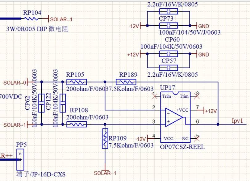
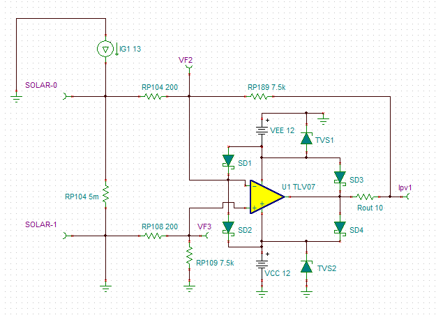
The schematic is as below. Ipv1 is connected to TL074TL074 forms a voltage follower, and the TL074's output is connected to the ADC pin of C2000.

It can work well during normal temperature.

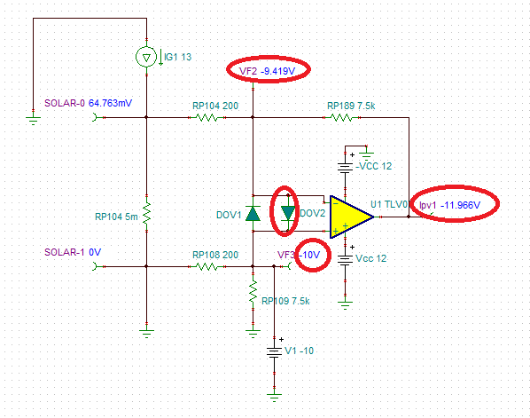
But at 70-80C, Ipv1 will be -12V, TLV07 pin 2 voltage is 0V, pin 3 voltage is -10V. 

At this time the boost will be turned down and their should be no current flowing through the shunt resistor RP104.

After cooling down the board, this phenomenon still exists.

After power cycle, the phenomenon disappear.

The failure rate is 4.1%.

Could you please provide any idea? 

  • Hi Howard,

    is there a mistake in the schematic arround RP109? How is "SOLAR-1" connected to "GND"? What is the voltage difference between "SOLAR-1" and "GND"?

    Your problem looks like latch-up and is caused by violating the common mode input voltage range in combination with a too high input current, e.g.

    Can you show us a bigger snippet of schematic?

    Kai

  • Solar-1 is not GND.
    The current sense resistor RP104 is connected between Solar-1 and Solar-0.
  • Yes, that's why I ask... :-)

    What is the voltage difference between "SOLAR-1" and "GND"? Can the potential of "SOLAR-1" violate the common mode input voltage range of TLV07?

    Kai
  • No, the sense resistor is only 5mOhm.

  • Howard,
    What is the differential voltage between SOLAR-0 and SOLAR-1, and what's the input common-mode voltage with respect to supplies When the problem occurs? Is this really 700V that I see?
    The way schematic is drawn will NOT work because the inputs seem to be floating with respect to system ground, which would result in the output collapsing on one of the rails.
  • Marek,
    Solar--1 ties to GND somewhere else in the circuit, so the common-mode voltage is almost 0.
    You can ignore 700V, it's comment of other circuit, not this one.
    The differential voltage between SOLAR-0 and SOLAR-1 should be less than 13A*5mOhm=65mV.
    The circuit can work well at room temperature.
  • Hi Howard,

    you wrote: "Solar--1 ties to GND somewhere else in the circuit, ..."

    But that's exactly the crucial point! Can you show us how and where "SOLAR-1" is connected to "GND"? If there is a longer copper trace with non negligible inductance involved, switchings can cause inductive kickbacks which can easily exceed the supply voltages of TLV07.

    Kai
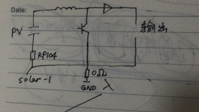
  • The main boost power stage is shown below, RP104 is shown there, solar-1 is connected to GND through 0 ohm resistor. Both Solar-1 and GND have large copper poured on the PCB on the same layer.

    So I guess there should be no big inductance.

    And this phenomenon could not disappear after power cycle. 

    OP07 from ADI with exactly the same circuit passed the aging test.

  • Can you confirm that the +12V and -12V power supplies are always there during the operation where the TLV07 appears to latchup?  I assume the real problem is customer expects 0V out for 0 current in but he sees -10V out instead. Do the 12V power supplies ever cycle on and off during operation?

  • Howard,

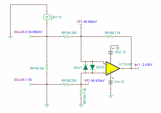
    Your customer's circuit should work just fine - see below.

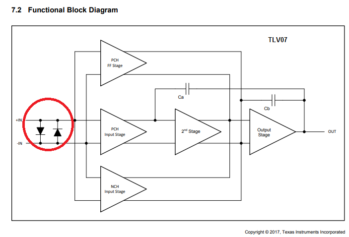
    However, your description of the failure, "at 70-80C, Ipv1 will be -12V, TLV07 pin 2 voltage is 0V, pin 3 voltage is -10V"  does NOT seem possible since there are internal protection diodes, DOV1 and DOV2, between the input terminals that should keep pin 2 and 3 to be within a diode drop from each other - see below.

    Having said that, your customer's problem seems like latchup condition or damaged device - does the part ever recover or not?

    If it does not recover, this seems like an overvoltage related damage and customer must add extral EOS protection circuitry as shown below.

    Schottky diodes, SD1 and SD2, protect the part from overvoltage on the positve input (for possible voltage spike on SOLAR-0) while transient voltage supressors, TV1 and TV2, prevent the damage due to excessive voltage on the supply pins that can be caused by spike on supplies and input voltage dragging the supply above absolute maximum rated voltage (e.g. LDO cannot sink current) or delay in power-up sequence between supplies (one supply is on while other one floats for few milliseconds).  If the customer drives inductive loads with a possible inductive kickbacks, they must also add SD3 and SD4 together with Rout current limiting resistor to prevent the damage to output stage - see below.  

    I have also attached in this post a short presentation with more ESD/EOS protection details.

    ESD_EOS.pptx

  • Marek,
    thank you for the timely feedback.
    Is the two diode between pin2 and pin3 is measurable with multimeter? We can't observe voltage drop like 0.3-0.7V with multimeter with no matter good device or the bad device detached from their board. So it's hard for us to tell whether the bad device pin2 and pin3 are damaged.

    Having said that, your customer's problem seems like latchup condition or damaged device - does the part ever recover or not?
    Yes, it can recover. Only by cooling the board it will not recover, but by power cycle the board it can recover.

    Since it can recover so we can the device is not damaged, right?

    If it's latchup condition, how can Vin+ be -10V? (We've observed with scope, it's a steady line at -10V so we are sure it is). What are the possible causes for OP amp to get into latchup condition?
    If it's damaged, so the voltage drop between pin2 and pin3 should be different between good device and damaged device, right?
  • Tim,
    yes, the real problem is the customer expects 0V out for 0 current but he sees -10V at Vin+, and the output Ipv is -12V.
    Do the 12V power supplies ever cycle on and off during operation?
    They haven't observed the power supply all the time with scope so we are not sure.
    But even if it cycles on and off during operation, will it cause -10V at Vin+?
  • Losing one of the supplies (one supply floats) may lead to a latchup condition if there are no TVS's on supply pins to provide the path for the quiescent current to flow from a positive to negative supply.

    There are back-to-back input protection diodes between the input terminals of TLV07 - see below.

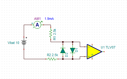
    The easiest way to measure the diode voltage drop in TLV07 is to pull the inputs apart with a voltage source, Vbat, and the internal 2.5k input resistors, R1 and R2, will limit the current to Iin=Vbat/5k - see below.  This way you may limit the current to 10mA or less by appropriately choosing Vbat supply - no need to power TLV07 supplies.  Under latched conditions, there may be another parasitic diode conducting the current and causing the problem your customer sees.  For that reason, they should add overvoltage protection I discussed in my previous post to prevent this condition from occuring.

  • Hi Howard,

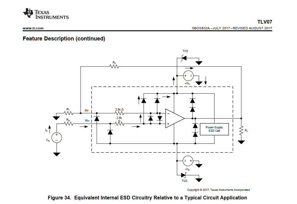
    you cannot directly measure the protection diodes between pin2 and pin3 because there are internal 2k5 resistors in series with the protection diodes:

    Kai

  • Howard

    We haven't heard back from you so we assume this answered your questions. If you need more help just post another reply below.

    Thanks
    Dennis
  • Marek,
    I've done experiment with the customer today.
    We found that the abnormal happens when pin2 or pin3 of TLV07 is touched by the probe of scope or multimeter.
    When pin2 is touched, the boost stage will stop working and the current sensed will be 0. Then the output of TLV07 is +11.8V, pin2 is -10.2V, pin3 is -11.8V.
    When pin3 is touched, the boost stage will stop working and the current sensed will be 0. Then the output of TLV07 is -11.8V, pin2 is -0.76V, pin3 is -11.8V.
    The TLV07 can't return to normal unless we power cycle the circuit or we touch pin2/ pin3 again.
    I also test by touching pin6. The boost stage will also stop working. But TLV07 could return to normal without power cycle or touch pin6 again.

    So the malfunction is not only caused by aging test, it should be related to interference signal on TLV07.
    Is this phenomenon like latch-up?
    Are there any way to make TLV07 not so sensitive?
  • Hi Howard,

    this sounds to be a layout issue. There seems to exist a lot of common mode noise between SOLAR-1 and the signal ground at UP17.

    The decoupling cap CP57 is close to UP17, right? Does the latch-up also occur if you connect the ground pin of multimeter to the ground terminal of CP57?

    Kai
  • This was taken offline to direct email.