This thread has been locked.

If you have a related question, please click the "Ask a related question" button in the top right corner. The newly created question will be automatically linked to this question.

TPS92661-Q1 layout desing

Hi,

On the TPS92661 package there are GND pin between each control io pin.

On the EVM each gnd pin is routed to an external connector

Can i route control IO pin without GND between them ?

(i assume that gnd pin is for thermal consideration)

(My board was a mcpcb mounting on heatsink)

Tanks

  • Hello Mederic,

    Let me move this to the LED driver forum, they should able to answer your question.

    Regards,
    Karl
  • Hello Mederic,

    The interleaved GNDs serve a couple of purposes.

    1. Because the part has been designed for use on single-layer MPCBs where routing density is often very high, the additional GND traces provide a lower impedance GND connection from IC-to-IC since there is no plane.

    2. The routing of the interleaved grounds provides some additional guard banding for the digital I/O. Although the primary benefit is just the increased space between traces and you will get roughly the same performance even if you delete the GND runs and leave the I/O spaced.

    The vast majority of the thermal conduction will be via the thermal pad on the bottom of the IC and that is not a primary consideration for the GND traces.

    You can certainly eliminate some of the GND traces from your design. They are not mandatory, but you may suffer a hit to signal integrity on the I/O. This is of course said without knowing anything about your design beyond the few sentences above.

    Best Regards,
    Mike
  • Hello Mike,

    Tanks for the awswer and the speed.

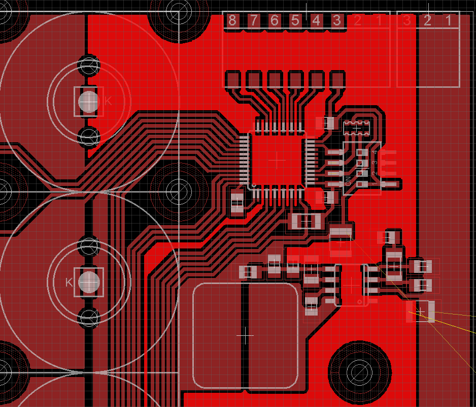
    There is a part of mi design with GND highlitghted (the board was a MCPCB)

    Do you think my GND trace was ok?

    Best Regards,

    Médéric

  • Hi Médéric,

    If you only have room for a single GND trace within the I/O routing, I would bring it off of pin 9 to separate CLK and TX. CLK will generally be the most problematic aggressor and TX is tri-stated when there is no read active.

    What is the other circuit shown in the lower right? That would appear to be maybe an inductor adjacent to the RX trace? Is this a switching regulator?  If so, that could create problems.

    Thanks,
    Mike