This thread has been locked.

If you have a related question, please click the "Ask a related question" button in the top right corner. The newly created question will be automatically linked to this question.

TPS50601A-SP: Output Ripple interpretation

Part Number: TPS50601A-SP

Customer has modified an TPS50601A EVM to look at his desired configuration: L = 5.6 uH, Cout = 2x18uF + 8uF, all ceramic. Vin = 5V. Fsw = 200 kHz

With output set to 2.5V, load = 250 mA, output ripple captured on scope: 

This seems reasonable.

When output voltage adjusted to 1.8V, (Iload = 250 mA), output ripple waveform looks like this:

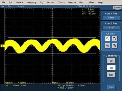
Amplitude of ripple (pk-pk) seems reasonable, but waveshape is different from 2.5V case. For example, the rise/fall times don't seem to align with duty cycle (36%), and signal appears "noisier". Any explanations as to why the different response?  

  • Hi Mark,
    What are your compensation components in the design that you are using.
  • Hi Mark,
    Looking further on your issue:
    In your application Vin = 5V, Vout = 2.5V @ 250mA and fsw = 200kHz.

    This will give you pk-pk inductor ripple current of 1.12A nominal & 1.395A max for 2.5V output and 1.0A nom. & 1.28A pk-pk ripple for 1.8V output Higher pk-pk current is due to 20% inductor variation.

    Output current will be average of pk-pk inductor ripple current ( as you have selected the proper inductor value) thus it show me that you very well understand the concept as a result have selected the proper inductor for the application. This is sometimes not clear to lot of engineers in various companies thus the importance of highlighting it.

    As output ceramic capacitor are used in your application. Ceramic capacitors derate with voltage. Thus I am assuming that you are using output capacitors that are at least 10V rated for the application and not voltage rated close to the application voltage. If ceramic capacitors are close to the actual voltage rating then capacitance can reduce as much as 70%.

    I think the waveform issue is more related to measurement. If you were to re-test the part and make sure that you are using a cold nose probe i.e. connection that has reduced ground lead connection the waveforms should look normal as expected in both cases.
  • Hi Ramesh,

    Thanks for the comments and vote of confidence on the design. We are trying to make a small sized solution, so the design has relatively high ripple current compared to the output load current to allow a smaller inductor (K>2). 

    I will pass along the recommendation on how to remeasure the ripple.

    By the way, here are the compensation values (selected using Webench). Rcomp = 301 ohm, Ccomp = 330 nF, Ccomp2 = 620 pF, Ccomp3 = 750pF.

    Also, speaking of compensation.  The Re-Comp feature of Webench shows the power stage response has a complex double pole instead of the expected real poles for the typical current mode control device.  This seems to be an artifact of the low values chosen for the Inductor and output caps, again to save space. The double pole makes it difficult to add much phase boost so phase margin is not as high as I like. Tests so far show the design to be stable and working as expected, except for understanding the ripple waveform at 1.2V (original post has an error. Output voltage at lower setting is 1.2V, not 1.8V). 

  • Mark,

    Can you let me know what is the DCR of the inductor that you are using as well as esr of the output capacitors. Or you can provide the part numbers of the two.
    Note one often overlooked conditions is if the DCR of the inductor is hish ( say 100mohm) and you do not have external current limit protection, thus you are relying on the TPS50601A-SP internal current limit which is about 10A nominal. Thus under overload conditions power dissipation in the inductor will be (I^2 x R) that would be about 100 x 0.1 = 10W . This will result in output inductor desoldering from the PCB. Not something one wants to see. Thus the reason on the TI EVM I have used inductor with DCR of about 5 m-ohm.
  • Hi Ramesh,
    Inductor: DCR = 30 mOhm, Isat = 2.1A
    Output caps: ESR = 6.3 mOhm each.

    It is understood that the circuit will probably not survive a short circuit event. To use an inductor with a high enough rating would have been too large to fit in the allocated volume for the design.

    Going back to the original question about the output ripple. I verified that the ripple is being measured properly using a tip/barrel method with the scope probe (no ground lead). Also, one correction to my original post. The first ripple response shown at Vout = 2.5V is with the EVM with the default components, no modifications. The second plot is the ripple with the target design components (L, Cin, Cout, Comp and Vout changes).
  • Hi Mark,

    As my initial thought was that if only thing that customer is changing is output voltage set point. Then I would not expect the output ripple waveform to change as shown.
    If you can provide the inductor part number as well as the various output capacitor part numbers. As the best way to address this would be to actually modify the EVM with the values used and see the issue on hand.
  • Hi Ramesh,

    Inductor: XAL7030-562MEB..

    I don't have exact PNs for the caps. I'll try to get better information.

    Here is how the EVM was modified for the testing:

    TPS50601Aevm mod.pdf 


  • Hello Mark,

    Sorry for the delay on the reply. I will be supporting this application moving forward. Is this an issue you are still seeing? If som could you let me know where you are with trying the suggestions Ramesh has previously mentioned?

    Thanks,
    Kyle
  • Hi Kyle
    I may need additional help on this. I will send you an email outside of the forum.