This thread has been locked.

If you have a related question, please click the "Ask a related question" button in the top right corner. The newly created question will be automatically linked to this question.

RE: Interfacing ADS5400 with Virtex 6 via a FMC-ADC adapter

Other Parts Discussed in Thread: ADS5294

Hi everyone,

I am working on 14-bit High Speed Serial LVDS ADC data (DDR) capture using ADS5294 EVM as my ADC and Zynq (ZC-7020) as my FPGA. Let me explain my requirements and problem to you guys.

I have developed hardware and software part I am able to send and receive simple bits pattern form ADC and receive it on my FPGA. Shifted version mostly i.e if I send 11111110000000 I my receive 00111111100000 or any other version of this. But when I send a signal I am not able to receive it correctly neither the shifted nor the correct signal. Like If I send RAMP (generated internally in ADC board) overall shape of received signal is like RAMP but some bits are missed or skipped. 

Scheme I have followed to design Hardware for capturing.  

I am following this guide for designing: 

I have made the exact figure 3-1. then I have combined DDR output to make a sample of 14 bits.  

Now the problems I am facing:

  • In this guide on page number 10 Figure 3-1. it is shown that BUFIO should be used after IDELAY to forward Bit clock to IDDR. but when I use BUFIO I receive error during routing. Error: "[DRC 23-20] Rule violation (RTSTAT-1) Unrouted net - 1 net(s) are unrouted. The problem bus(es) and/or net(s) are design_1_i/iddr2_ip_0/inst/cBufferedIO."  And Is it necessary to use BUFIO here or not?
  • And what can be the problem for not receiving the RAMP correctly.

Regards

  • Hi,

    the ADS5294 is not supported in the High Speed Data Converter forum, as that device is supported by the Medical group in their forum - even if the end application for the device might not really be medical.  They are the ones who know the device.   I will split this thread and move this portion over to that forum.

    I would say that you should use whatever buffer the FPGA vendor recommends for clocking the IDDR cell.   The FPGA provides IDDR cells that are specifically made for latching in data on rising and falling edges, and also they provide the IDELAY cell on each input so as to be able to delay either clock or data as needed to meet setup and hold time into the IDDR cell.   Whatever method the FPGA vendor recommends to get the clock to the IDDR cell is what I would go with.  

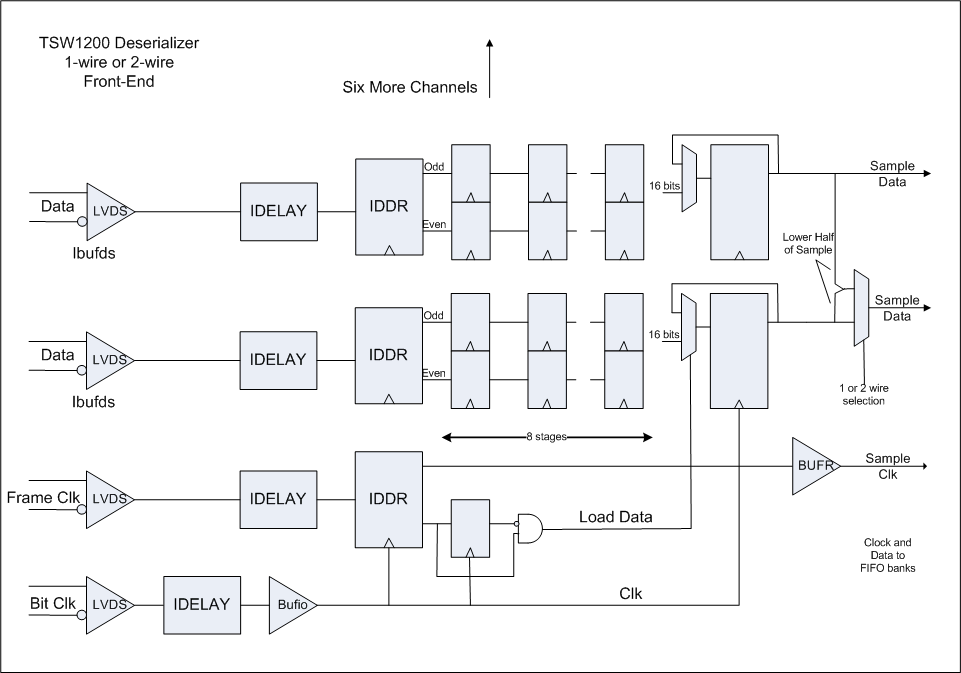
    Now that figure 3-1 simply shows the most basic circuit to get the data latched into the FPGA.  In the case of an ADC with a parallel bus of data, the data out of the IDDR cells is the sample data and the buffered version of the clock is the sample clock into the fabric of the FPGA to go with the data.   In the case of an ADC with serialized data such as the device you are looking at, after the IDDR cell you do not yet have a whole sample - only two bits of the serialized sample.   You still have to at that point keep latching in more data until you get a whole sample and have a way to chop that serial data stream into a stream of whole samples.  The figure 2-1 is one such mechanism to do this, but using the frame clock to latch the whole sample is tricky to get the timing right as shown.  Other people may use an ISERDES element instead of the IDDR.  What I did to get the deserialized data latched into a whole sample is as in the attached sketch - I used a latched copy of the frame clock to mux the data streaming through the deserializer into a sample register once per frame clock.   But after that you still have to buffer the frame clock into the fabric of the FPGA to become your sample clock using whatever buffer the FPGA tools allow you to use (maybe not a bufio).  And you have to be sure that your design will close timing using the FPGA vendor's static timing analyzer tool for the sample rate you wish to run at.

    Regards,

    Richard P.