This thread has been locked.

If you have a related question, please click the "Ask a related question" button in the top right corner. The newly created question will be automatically linked to this question.

DRV8332DKD mismatch between datasheet, package drawing and actual package

Other Parts Discussed in Thread: DRV8332

Hello,

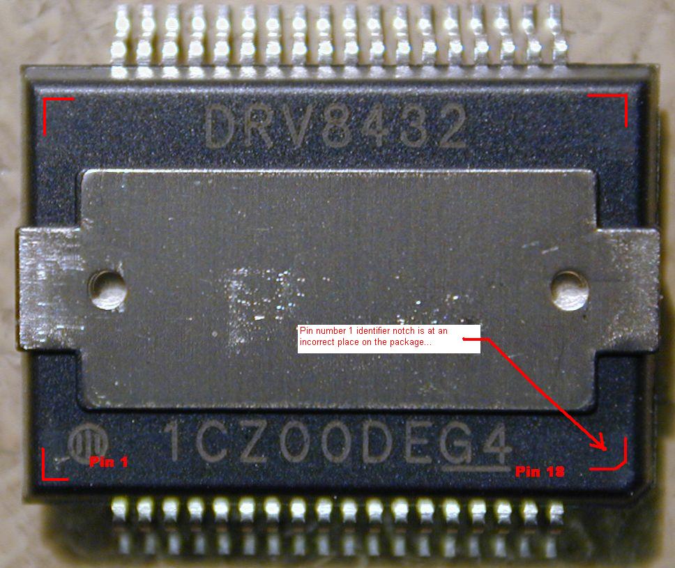
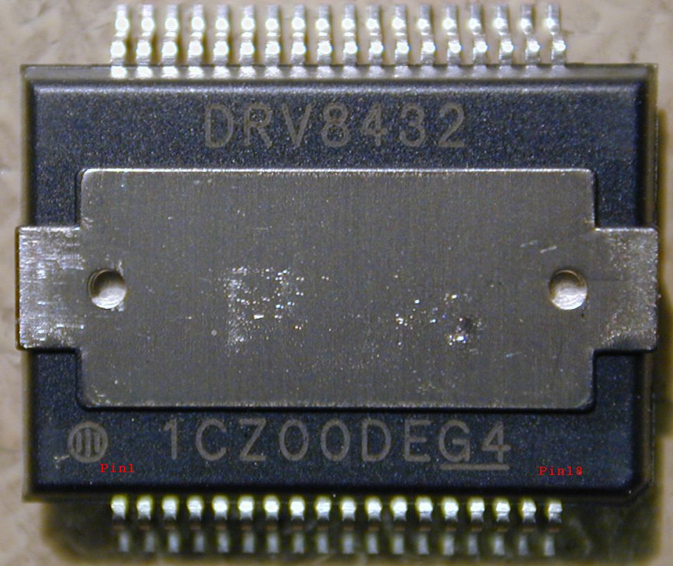
my question could looks like a stupid one but I have some problems in finding the right placing of the DRV8332 DKD. It seems I'm not able to find the pin nr .1

First of all I think there is a mistake in the datasheet of the IC as the package drawing (page 27) is different from the one shown in the doc. "mpds126h.pdf".

If we assume the right drawing is the one in the doc. "mpds126h.pdf", then I think there is another mistake in the datasheet on page 4: here the top view of the DKD package, doesn't match with the package drawing of the pdf file.

Finally, the DRV8332 samples I have received don't match with no one of the above situation as the pin nr.1 seems to be the top left one.

For better explanation I have attached a file with some pictures.

I hope somebody can help me asap as I need to assembly my board.

Thanks

Massimo Zangoli

DRV8332 Package issues.doc
  • You are not stupid, it is stupid that it should be necessary to ask! And my experience is that TI FAE's have problems figuring this out too.

    The conclusion so far for me is:

    The corner notch is not pin 1. The indentation is not pin 1. They are both pin 18. This is a first for me in 30+ years!

    The pin 1 marker is actually the printed O with 3 vertical bars in it. I'll se if I can attach a picture. Note the Notched corner is in the opposite end of pin 1.

    This information is to my best understanding what I was told by TI representatives. I am not a TI employee, so my info here is not official!

    (And my parts still don't work. Neither do they emit smoke or sparks.)


  • All,

    There was an error in the datasheet that creeped in to a recent revision of the datasheet.  The package drawing incorrectly shows the pad exposed on the bottom of the package.

    This was corrected in the DRV8432.  The packages are the same between the 8332 and 8432, so please follow the package drawing in the 8432 until I can get this fixed.

    http://www.ti.com/lit/ds/symlink/drv8432.pdf

  • Hi Ryan, Hi Massimo and Hi Einar,

    I was planning to use DRV8332DKDR in one of my design but after reading Massimo's and Einar's posts and looking at the photos in these posts, I am confused to use DRV8332DKDR. Yes, Ryan, you are right that there was an error in the previous datasheet (see the attachment : TI - erroneous - DRV8332DKDR and DRV8312DDWR.pdf) on page 27 as the heat slug is shown on the bottom of the package. And I can see that this error is corrected in the latest datasheet as the heat slug is shown on the top of the package (see the attachment : TI - corrected - DRV8332DKDR and DRV8312DDWR). But there are still problems as seen in the photos sent by Massimo and Einar. So Ryan, my questions are:

    1) Was there a problem in the package of DRV8332DKDR (and also in the package of DRV8432DKDR) in the first productions of these integrated circuits?

    2) Will TI guarantee to send the correct package of DRV8332DKDR with heat slug on the top and pin number 1 identifier notch on the correct place?

    3) If I request DRV8332DKDR and if I receive the package as shown on the attachment Einars_IC_photo.jpg, should I accept Pin 1 as Einar shown it on the photo although the pin number 1 identifier notch is not on the correct place? (By the way, Einar I have included a small note and several lines on your photo in order to clarify the situation).

    Thank you very much for your attention,

    Zeynel OLGUN

    4807.TI - erroneous - DRV8332DKDR and DRV8312DDWR.pdf

    8372.TI - corrected - DRV8332DKDR and DRV8312DDWR.pdf

  • 1)  There is no problem.  The notch is the correct pin one indicator for "pad down" packages.  For the pad-up, it is in the wrong location. 

    2)  To my knowledge, the notch will remain in the current place as the picture you attached shows.  The pin 1 indicator is the circle with 3 lines in it. 

    3)  You notations in the picture are correct. 

  • OK Ryan, I will accept the pin nearest to circle with three lines inside as pin 1.

    I won't take into consider about the corner notch.

    Thank you.