This thread has been locked.

If you have a related question, please click the "Ask a related question" button in the top right corner. The newly created question will be automatically linked to this question.

DRV8313 evm R1 resistor removed

Other Parts Discussed in Thread: DRV8313

Hi,

I'm trying to drive the DRV8313 evm with an external microcontrolleur (ezdsp F2812) and there is some Zero-ohm-Jumpers that should be removed before(R25,R26,R27,R29 and R30 to R34), but when i tried to remove this jumpers i accidentally removed another resistor ( R1 ) which is not supposed to be removed

i want to know is this could have any consequences on the working of the board

best regards  

  • Hi Sadok,

    R1 is the pull up resistor for nFAULT. nFAULT is an open drain output. If you are not monitoring nFAULT in your firmware you should be ok without this, though I would recommend soldering it back so that you can see FAULTs.

  • Hi

    Ok for the moment i'm not using the nFAULT signal in my program, i' just trying to run my brushless in open loop (without feedback from hall sensors)

    i just programmed the logic table (i found it in the datasheet of the DRV8313 ic ) ans it should achieve standard 120° commutation , so my ezdsp produce the six signal correctly and i visualized them and normally everything is correct

    after that i've connected my six signal in order (IN1,EN1,IN2,EN2,IN3,EN3) to the J1 header's first six pins and i putted high the ninth and tenth pins of J1 witch are RESET ans SLEEP but i don't see anything in the output's phases (of course my drive is alimented in 12 v )

    can anyone help me with this ?

  • Hi Sadok,

    Would you please check your ground connection from your micro and the source of the two high inputs to RESET and SLEEP? If there is no common ground this could explain the behavior.

    If ground is correct, please try a simple experiment using IN1 and EN1. Connect IN1 and EN1 to a logic high and verify that the OUT1is at VM. Then set IN1 to a logic low and verify OUT1 is at ground. If OUT1 is not following IN1, this appears to be a problem with RESET/SLEEP. If it does follow IN1, this appears to be a problem with the microcontroller connections.

    This will indicate if the RESET and SLEEP connections are working properly. This can be repeated on IN2/EN2 and IN3/EN3 if necessary.

    Please do not post the same question in multiple threads. I will update the other post to note that it was answered in this thread.

    Thanks.

  • Hi Rick

    Yes, i forget about the ground connection but even when i established a wire between the AGND of the ezdsp and the ground of the drive nothing is changing

     The signal for the RESET and Sleep are both generated from the dsp too, and i tried now the experiment to test the first output (OUT1), i have putted IN1, EN1, RESET and SLEEP on high logic  (the amplitude of the signal generated from the ezdsp is 3.3 v ) and i didn't forget to make the ground connection between the two boards and still don't have the output signal

  • Hi Sadok,

    It appears like you will have to dig a little deeper.

    When you set the IN1/EN1/RESET/SLEEP to a logic high, please measure the voltage at TP1 and TP3 (IN1 and EN1). If the micro is not using a strong enough drive, the internal pulldown on the pins could prevent proper operation. 

    Then, please add R1 back on the board. Next, set RESET and SLEEP to a logic high and measure and report the voltages of the following pins:

    V3P3OUT
    FAULT
    VCP

    These signals will determine the next step. If V3P3OUT is 3.3V and VCP is approximately 22V, the device is awake and FAULTn could be interfering with operation.

    If FAULT is low, the cause of this will have to be determined. With no motor being driven, FAULTn low is unlikely but cannot be ruled out.


  • Hi Rick

    thanks for assisting 

    but now i'm testing the TP1, i can't find my 3.3 signal but the signal is well generated from the dsp , when i disconnect the rubon cable and i mesure it , the signal is established but once i connect the two boards i can't find the signle any more (that's strange ), but the signal TP3 is ok, i fond it even when the two boards are connected !!!

    (i verifed all the wires and connections and they are well installed )

    have you any explanations ?

    best regards  

  • Hi Sadok,

    This can be related to the settings on the dsp. Since I don't know how your firmware is written, I can only speculate at this point.

    Some GPIOs on various micros can be set to provide different drive strengths. If the drive strength is too weak, the internal pulldown can prevent the dsp from driving the signal to a logic high.

    What exactly are you seeing when you say you cannot find the 3.3v signal? Are you measuring with a DMM or a scope? Can you provide screenshots if using a scope?

    I suggest you remove the dsp from the equation. Try connecting IN1/EN1/SLEEP/RESET to an external 3.3V supply through a 3.3k resistor. Then measure TP1, TP3, V3P3OUT, VCP, OUT1, and FAULTn and report the voltages.

    This should give the most information.

  • Thanks

    It's a little bit strange but when i tried the same procedure but with IN2,EN2,RESET and SLEEP,it make sense. With this configuration i mesured TP4 and TP5 and i found my 3.3 v signal on both (with DMM), ans also i measured  V3P3OUT signal , it has 3.3 v like value , VCP is 12 v (i'm giving 12 v supply on VM ? it's the same as VCP because i can't find VCP on the board) , for FAULTn , the signal is low(0 v), the OUT2 is also low 

    i didn't replace R1 resistor yet, because i lost it , in case i should replace it could you give me the value (or part number for it )

    best regards 

  • Hi Sadok,

    Was the procedure for IN2/EN2/RESET/SLEEP exactly the same as IN1/EN1/RESET/SLEEP? Did you use the same signals to drive both IN2/EN2/RESET/SLEEP and IN1/EN1/RESET/SLEEP? If you did not, please use the same signals for both sets of inputs.

    Is it possible that there is a solder bridge on the pads of the resistors you removed? This could cause unexpected problems as well.

    If VCP is 12V, this means that charge pump is not operating properly.

    The nFAULT will read 0V because the 5k pullup resistor R1 is not installed. Once it is re-installed the voltage on nFAULT will indicate if the device is actually faulting.

  • Hi Rick

    Yes the procedure was the same, the signals was the same , so i can conclude that the problem is not related to the dsp signals

    concerning you second remark i don't know exactly, because it wasn't me who has removed the resistors, i've a gave the board to  a friend and after he gave me back the board i realized that heommited R1 resistor (i didn't demand that !!)

    For the VCP where can i mesure it (can you precise the location on the board because i can't find it )

    another thing , i have connected IN1/EN1/SLEEP/RESET to an external 4.5 V and the signal i mesured were :

    - TP1,=TP3=0 v

    -V3P3OUT=0v 

    -IN1=IN2=IN3=9.5 v 

    remark , i connected the four signals directlu not through the 3.3k resistor like you proposed  

    i will try to replace the resistor next week and i will try again 

    best regards 

  • Hi Sadok,

    You seem to be missing one important source of information. Please go to http://www.ti.com/tool/drv8313evm There you can find both the user guide and a zipped file under the Software heading. The zipped file contains the board schematic and layout which will help you performing debug.

    The results you are reporting are inconsistent. TP1 and IN1 are the same net. How can TP1 = 0V and IN1 = 9.5V? If you are really measuring 9.5V on TP1, TP4, and TP6, the device has been damaged.

    V3P3OUT = 0V indicates that either VM is not applied to the DRV8313 or that the device has been damaged. When the DRV8313 is powered up, V3P3OUT (TP2) should measure approximately 3.3V.

    Please apply 12V (VM and GND) to connector J2 and measure the voltage at TP2 (V3P3OUT). If the voltage is not 3.3+/-10%, the device may have been damaged. If it is within the 3.3+/-10%, the next step is to proceed with additional debugging. What equipment do you have available; DMM, resistors, clips, etc?


  • Hi Rick

    I'm really sorry , it was just my Fault , i meant  OUT1=OUT2=OUT3=9.5v and not IN1=IN2=IN3= 9.5 v 

    i was clumsy when writing my last reply 

    excuse me , i didn't meant that

    i don't know may be the guy that has handled the boards has damaged it 

    For the equipment i have the necessar ones i thought 

    i will try to find someone to replace the R1 resistor and see 

    best regards

  • Hi Sadok,

    No worries. That explains some of the inconsistent data.

    There is still more inconsistent data however. OUT1 = OUT2 = OUT3 = 9.5V indicates that the outputs are powered up and running. V3P3OUT = 0 indicates that the device is in not operating. It should be operational for the device to provide 9.5V on OUT1/OUT2/OUT3.

    Also, TP1=TP3=0 v when IN1/EN1/SLEEP/RESET are connected to 4.5V should not occur. As mentioned TP1 is the same net as IN1, so both should measure the same value.

    Do you have something connected to OUT1,OUT2,OUT3? If you do, please remove connections to OUTx.

    Please apply 12V (VM and GND) to connector J2 and measure and report the voltage at TP2 (V3P3OUT). If the voltage is not 3.3V+/-10%, the device may have been damaged. If it is within the 3.3V+/-10%, the next step is to proceed with additional debugging.

  • Hi Rick 

    thanks for being so patient

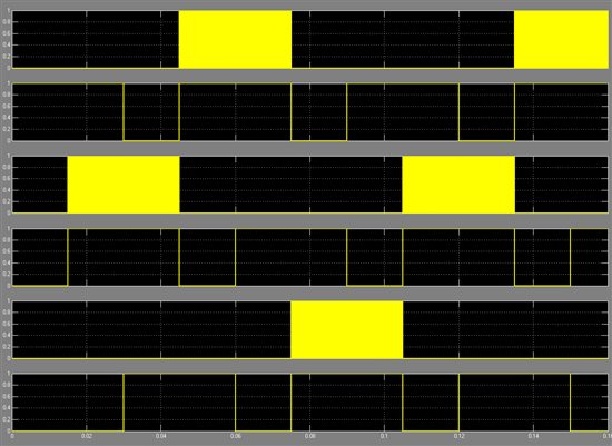
    So, i don't know what happened exactly but now i'm measuring 9.7 or 10 v on the three output of the drive (my VM is 12 v ) but the TP2   is always 0 v .the signal i'm generating from the dsp to the 6 first pins of  J1 are in the screenshot below 

    so the first signal is IN1 and the second is EN1 , same logic for the other signals

    the wide band you see in the inputs signals are a pwm signal with a frequency of 20Khz

    my question now is about the signals from the hall sensors , should i put them on the drv 8313 evm and the gate's  inverter will switch automatically or should i read this signals on the dsp and consider that in my program, because that,s is note mentioned is the datasheet of the drv 8313 

    thks 

  • Hi Sadok,

    It appears like the board may be working now, although it still is suspect. Would you please capture a scope shot of OUT1 when you are driving IN1/EN1 as shown above? Thanks.

    In addition to the schematic and layout, the zip file also includes the firmware for the MSP430 on the EVM. It is located in the folder "Board files" and is named "DRV8313_Firmware_Release" This file contains the code to control a BLDC motor using the MSP430.

    Please note that the HALL_x inputs are read by the MSP430, then translated to INx and ENx. This is what is required to run the motor. The HALL_x inputs designated when it is time to advance to the next step, and the microcontroller acts upon this information to output the next step signals to the DRV8313.

  • Hi Rick 

    What i'm trying to do is to read the hall sensors signals with the ezdsp F2812 board through the analog interface and use this signals to generate the adequate signals for the drv8313 evm, (i need your opinion concerning that ) 

    So my question is how can i read this 3 analogs inputs (hall sensors signals) ? i just have to put directly this three signals on the analog interface or should i put some intermediate components between the motor and the dsp pins (some resistors may be )

    Just to know , i'm using matlab simulink with code coposer studio to generated  code for the dsp 

    best regards   

  • Hi Sadok,

    What is the voltage output of the hall sensor signals? Typically there is a pullup resistor that sets the high voltage and the low voltage is approximately 0V. If your system is powered up without the motor windings connected, you may be able to rotate the motor by hand and examine the hall sensors as they change state.

    If the voltage of a logic one and zero is within the rating of the dsp, it can be read directly by the dsp to determine how to drive the INx/ENx signals. If not, it may require some conditioning to meet the voltage requirements of the dsp.

  • Hi Rick

    The Hall sensors signal is a digital signal , the amplitude of the signal is +5v , is it in range ?

  • Hi Sadok,

    I am assuming that the hall sensor signals will be connected to the ezdsp. In this case, it is a question of the maximum ratings of the ezdsp. Look at the specifications of the ezdsp and determine if it can handle 5V. I suspect it cannot.

    If it cannot, reduce the voltage to the ezdsp to meet the specification.

    FYI, the DRV8313 can accept 0 to 5.25V at the logic level inputs.

  • Hi Rick

    it's ok , i found the answer in the SPRAAP6A :

    • The voltage applied to the ADCIN pins should be restricted between 0 V–3 V. If it exceeds this limit on
    any channel, it temporarily affects the conversions on the other channels. If the signal conditioning
    circuit used for the input analog signal needs to use any higher supply voltage (i.e., 5 V), it is
    recommended that a buffer stage that scales this signal to < 3 V be used before connecting to the
    ADCIN pin.
    • If you need to monitor DC voltages higher than 3.0 V, the resistor divider should be followed by an
    op-amp buffer stage. By connecting the resistor divider directly to the ADCIN pin violates low source
    impedance requirement and conversion counts will see large errors

    best regards 

  • Hi Rick

    Is it normal that i measure 9.7 v on the three output of the drv8313 evm when i don't have any hight input on the J1 connector (input pins and enable pins ...), the dc supply is 12 v 

    is the board damaged ?

    thanks 

  • Hi Sadok,

    I don't think the board is damaged. I have seen this behavior with a similar device. I am trying to confirm that this device behaves the same way.

  • Hi Rick

    I was trying to test my drv with a simple, 1 phase, dc motor (i tryed the 3 outputs one by one) , the motor is running correctly but the problem that i can't control this output, it is always active even when you don't have any signal in the J1 connector I've putted 4.8 v on EN1, IN1, nreset and nsleep but it doesn't change anything , i tryed to remove some signals and keep some others but this doesn't have any effect on the output (it's the same case for the three channels)

    So please , just try to confirm what should be the behavior of the drv with the configurations above? am i giving the wrong control signal ? may be i should put the others free pins of the J1 in low state? 

    i'm really confused and don't know what to do 

    thanks 


  • Hi Sadok,

    I don't have a working EVM at the moment. I have ordered one and will check it in a few days when it arrives.

    In the interim, please try the following at report your findings.

    Place a 1kOhm resistor to GND on the outputs and measure the output voltage when nothing is connected to the inputs. I think you will find that the voltage drops to less than 1V indicating that the output is not active when the inputs are floating.


  • Hi Sadok,

    I did similar experiment with DRV8313 EVM. I made all the 8 control inputs of DRV8313 IN1/2/3, EN1/2/3, RESET and nSleep floated by removing corresponding zero ohm jumpers but did not observe any sign of high voltage at outputs, all the 3-outpus are zero. I measured the all the control input also to be at zero voltage. This is expected as per device data-sheet behavior because all the inputs have internal pull-down so floating them shall make all inputs to be low.

    I think in your set-up, some of the control signals may be high in floating state which is causing high voltage at output. I would suggest you to measure the voltage level at control inputs in floating state or when you try disabling the motor, this will provide us some clue on what exactly happening with your EVM?

    Best Regards

    Milan

  • Hi rick,

    I tried the  experiment you've recommended (Place a 1kOhm resistor to GND on the outputs and measure the output voltage when nothing is connected to the inputs) to me and the report is the following:

    -For the first output, i measured 8 v , the supply voltage is 12 v

    -For the second and third output, the voltage drops to less then 1 v like you've predicted, it's almost 0 v 

    so as you can notice , the outputs are not the same for similar input conditions

    thanks 


  • Hi Milan,

    As a preliminary observation, i can say that we don't have similar outputs measurements for similar input conditions and i measures TP1, TP3..TP7 they are all low voltage, in despite the three outputs were hight voltage almost 9.5 v but when they are not connected to any load 

    i will order a new board and see, i think that something is going wrong with the board ?

    Best Regards

  • Sadok,

    As Rick pointed out, it may not be bad device. There is possibility some smaples shows the high voltage output issue as you are observing.

    At my end I will try to repeat the test on few samples that are with me and share the findings. Please allow me couple of days to do the experiments.

    Best Regards

    Milan

  • Sadok,

    I repeated the test 3 more samples but none shows high voltage, all 3 outputs are zero. Based on this experiment, I think your sample might have damaged. As you already planned, I would suggest you to change the device or board and repeat the experiment.

    Best Regards

    Milan

  • Hi Rick, Hi Milan

    My new drv8313 was delivred today and i have tested it with the software of ti (i didn't remove the resistors yet ) and it works properly with ti software 

    Now i will need to remove the resistors so that i can use it with the external control signal from the dsp, so what precautions i should take into account before doing that, since that the first board got damaged when removing the resistors as i thought 

  • Sadok,

    Not anything specific, just make sure while removing the jumper resistors you do not over-heat  other components on board.

    Best Regards

    Milan 

  • Hi Rick, Hi Milan 

    First of all thanks for all this explanations, and like we have predicted the problem was with the old drv because once i have  changed the drv , my motor is running and everything is normally working.

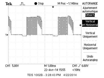
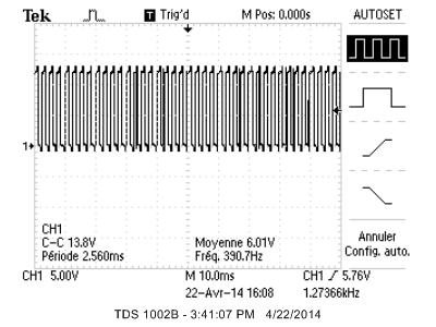
    but there is something that looks strange for me  (may be i'm not understanding it very well) , in fact i'm using pwm signal to fed the coils of the motor (with a frequency of 20 kHz) , when the duty cycle is 50 % i measured a voltage average of 3.8v ,the supply voltage is 12 v, the figure below is the screen shot for the output phase voltage 

    this figure below is for 100 duty cycle , the average i measured is almost 6 v

    thanks for any further explanations

    Best regards 

  • Sadok,

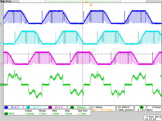
    There is something worng with the first waveform. It's not expected results, rising back-emf portion is absent from waveform.  Typically this happens when:

    1.  motor Hall-signals are not aligned properly with PWM logic , if  sensor are used

    2. or Commutation is not  matched  with back-emf zero crossing  in sensor-less algorithm. I am attaching the scope-shot of phase voltage waveforms, you should  get  the same results to achive correct commutation.

    Best Regards

    Milan