This thread has been locked.

If you have a related question, please click the "Ask a related question" button in the top right corner. The newly created question will be automatically linked to this question.

DRV8312 OUT signal is not correlated to the input signal

Other Parts Discussed in Thread: DRV8312

Hi,


the last days I tried to get a BLDC motor working. The circuit is derived from a former version, which works fine. So there is no generic problem with it. However, I needed to replace the power stage with the compact DRV8312 stage.


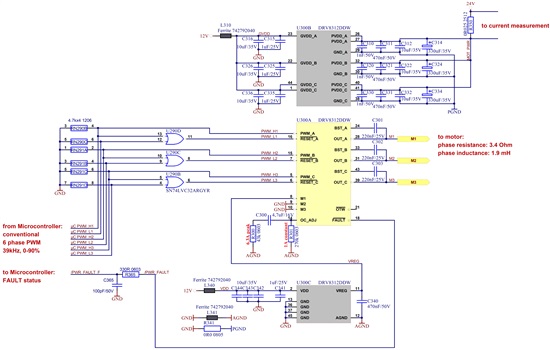
This is, how the stage looks like:

(Please click picture or refer to the attaced PDF for better wiev.)

The motor runs at 24V. So this node powers PVDD_x. There is a cascade of descent decoupling for each phase and the voltage has very low noise. All grounds and supplies are separated in their respective place and connected to system ground an power via 0R resistors and ferrites.

The "or"-solution comes straight from the datasheet. The only strange thing I did is to modify the OC adjustment. I need much power while speeding up the motor. So I set the peak limit to 6.3A (43kOhm). A capacitor limits the time of this peak current. The DC current is set to 1A (270kOhm). As this value is a little high, I also tried 200k.

The motor has a phase resistance of 3.4Ohm and its inductance is 1.9mH per coil.

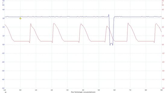
Seems like this circuit could be no problem at all. However, it does not work as expected. Please have a look on the input an output signals:

Please note, that the output was sampled with a 10x probe.

The microcontroller sends perfect signals at 38kHz (90%) to the DVR8312 PWM_A. PWM_B is low and Reset_B is high, so lowside should provide a ground path. However, OUT_A just goes into "Bootstrap Capacitor Under Voltage Protection", I think. The current through the motor is rather low, just a few Milliamps. The voltage at the bootstrap pins peaks up to 33V, which should be perfectly ok.


Anyone out there, who has an idea, what's going wrong here?

Every hint is much appreciated!

Thanks to everyone, having a look on this!

Ralf

DRV8312-signal-problem.pdf
  • Hi Ralf,

    Can you clarify a couple of items?

    What signals are shown in the scope capture?

    The OC_ADJ connection is not a recommended connection. For now, I suggest you remove it and increase the 270k resistor to 43k. This will allow focusing on one problem at a time.

    Once you make this change, would you please capture the PWM_A, BST_A, and OUT_A when attempting to run the motor? If you have a current probe, please capture the current through the motor also.

    Thank you.

  • Hi Rick,


    I have tested the OC_ADJ with some other values from 200k downto 43k and the output looks exactly the same.

    For better interpretation of the graph: The "good" blue digital signal is the PWM_x stimulus into the driver. And as the datasheet gives the or-ing solution, the blue signal is the RESET_x as well for my circuit. The red strange signal is the OUT_x signal.

    Today I tested a few other duty cycles. The output follows the input from 0-70% on time. Bigger values result in the jittering high frequency peaks shown in the red trace.

    I tried to hard-wire one state:

    PWM_A: GND

    PWM_B: GND

    PWM_C: PWM, 40kHz

    #RESET_A: GND

    #RESET_B: 3V

    #RESET_C: 3V

    This produces a stable OUT_C over 0-95%.

    The only difference so far is, that the circuit in Fig. 10 of the datasheet makes the output not toggle between PVDD and GND like in my hard-wired test. With the or-ing solution, it toggles between PVDD and HiZ. So the part of the question regarding the strange extra cycles is now answered.

    With the stable hard-wired setup, I tried to eliminate the influence of the motor. I just used a wire-wound resistor instead. Connecting it between any two of the tree OUT_x the circuit did not draw any current. This is why I do not attach a graph. It's just flat at almost 0.0mA. When connecting it between OUT_C and GND, I could modulate the current perfectly via the duty cycle.

    So, obviously the OUT_B does not turn on the low-side transistor. Measuring the voltage with the resistor connected shows no drop at all. OUT_B and OUT_C voltages are the same.

    I checked the soldering quality but that's fine. For noise reduction, all high current signals have a separate solid power and ground plane. This is power ground wired to the global ground via two soldering junctions. They are fine as well. I also tried another identical assembly. No success.

    By the way: The circuit is very compact. So all capacitors are more or less directly at the IC pins. I avoided vias. Just the bulk capacitors with 330µF each are on bottom. However, they are located directly at the IC as well. So no ringing or other oddities might happen here.

    Could you please help me with this?

  • Hi Ralf,

    Please note in your schematic, the M3,M2,M1 configuration is a reserved configuration. M3 should be connected to VREG. Sorry I missed this in the first pass.

    Once that is corrected, please focus on getting OUT_B working. The connections show it should work. I suggest you create a resistor divider from PVDD to ground and connect the mid point to OUT_B. You can easily determine if the output is low, high, or floating by driving the PWM_B and RESET_B lines as desired.

    Since multiple boards and multiple devices are showing the same behavior, I am hoping the mode pins are the reason. If not, it may be the layout.

  • Hi Rick,


    indeed, during design I just mixed the mode pins while tidying up the schematic. Directly after setting the mode correctly all boards are working fine.

    Thanks a lot for your help!

  • Hi Ralf,

    Glad we could help, and that it was a simple fix.