This thread has been locked.

If you have a related question, please click the "Ask a related question" button in the top right corner. The newly created question will be automatically linked to this question.

DRV8301-69M-Kit, issues with high duty cycles (PWM)

Other Parts Discussed in Thread: DRV8301-69M-KIT, MOTORWARE, DRV8301

Dear e2e-community,

I am using the DRV8301-69M-Kit with Motorware version V1.01.00.16. I developed an application based on project lab04. In this application I want to assign three pwm duty cycles manually. For this purpose I write the values

Tabc->value[0] = _IQ(dutyCycle0); 

Tabc->value[1] = _IQ(dutyCycle1);

Tabc->value[2] = _IQ(dutyCycle2);

This procedure works fine for a wide range of duty cycles. However, there are scenarios when it does not work as intended. Let me explain one scenario:

If I assign the following values by the debugger

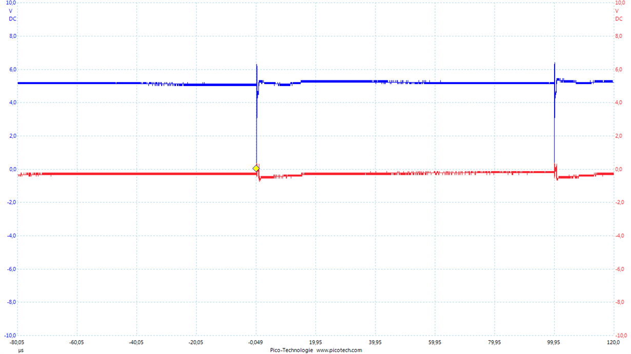
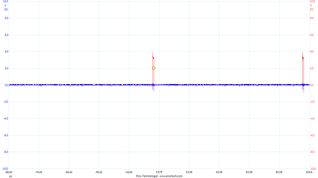
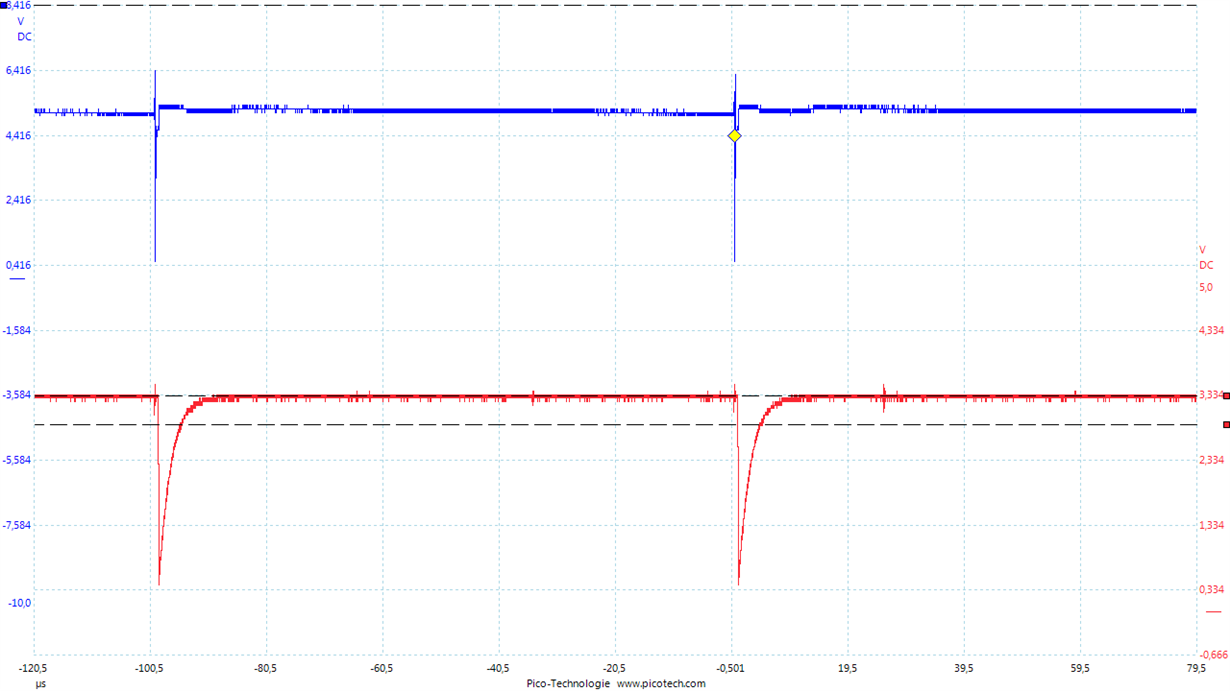
dutyCycle1 = 0.0 (red line)

dutyCycle2 = 0.4, (blue line)

and measure the output potential of the corresponding half bridges, the behaviour is correct and as expected:
However, if the value dutyCycle2 is changed to

dutyCycle2 = 0.497

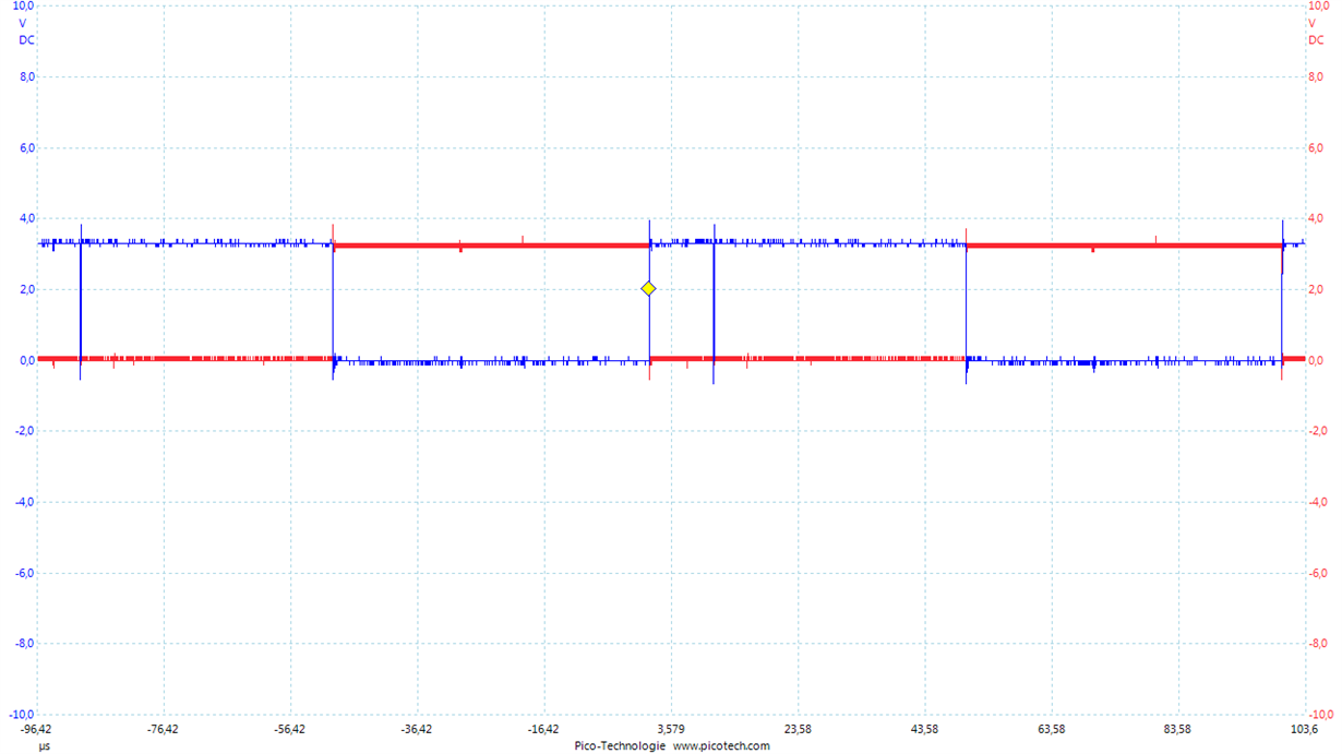
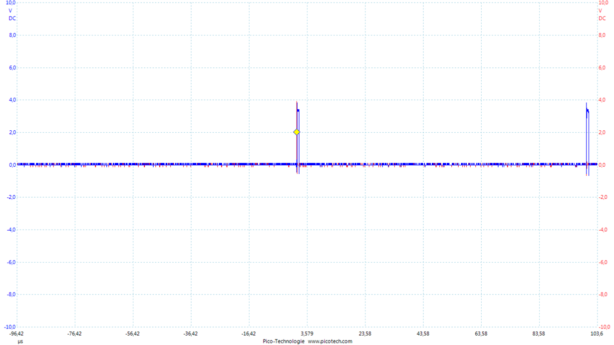
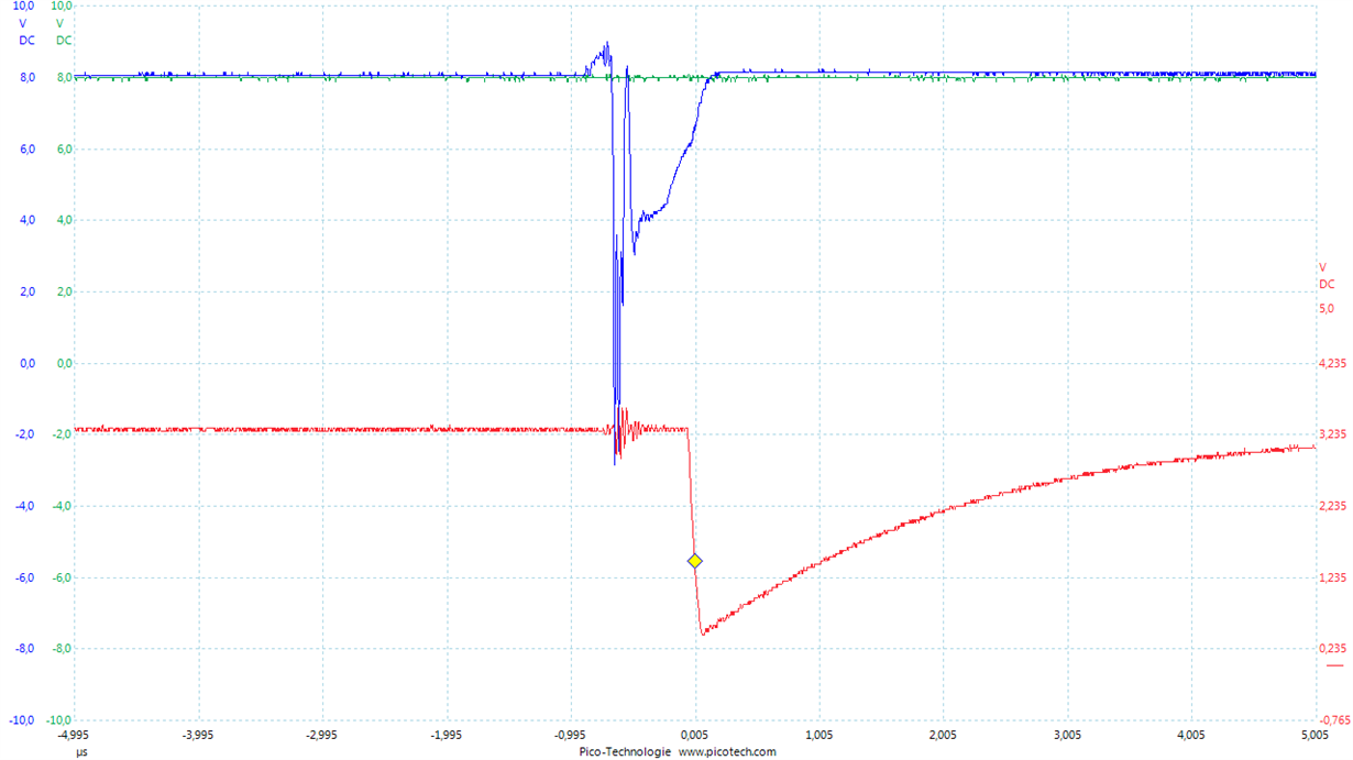
I observe an erroneous behaviour (output voltage of half bridge 1 is permanently low and the output of half bridge 2 is permanently high):

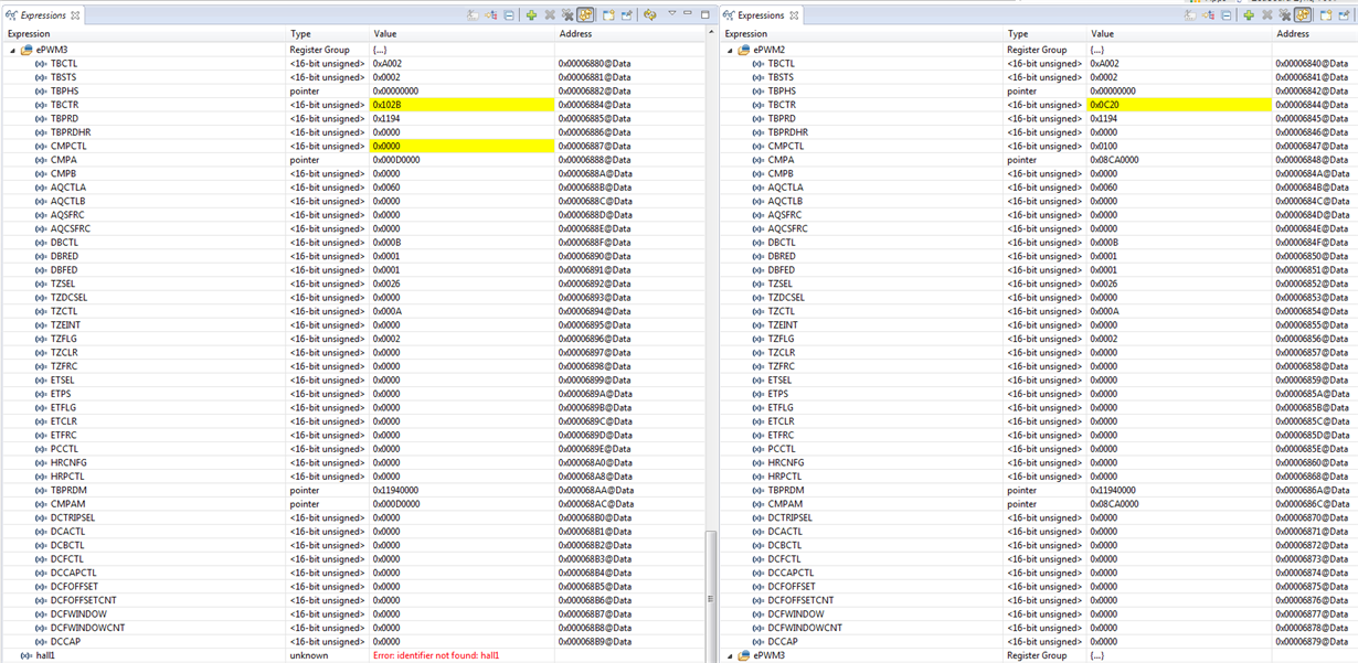
Please find the content of the ePWM registers (ePWM2 corresponds to half bridge 1 and ePWM3 corresponds to half bridge 2) below:

Why does the duty cycle assigned to half bridge 2 affect the (measured) duty cycle of half bridge 1?

Kind regards,

Oliver 

  • I'm seeing if a PWM expert can help address your question
  • Oliver,

    I don't have a complete answer for you but I can tell you there is nothing in the way you have the PWM configured which connects the duty cycle of one module with that of another.  I don't see anything in "hal.h" which does that either.

    I can see from the registers that you have 0x2 in the TZFLG register on both modules.  This indicates both PWM2 & PWM3 have received a trip input and that the trip was configured in cycle-by-cycle mode.  My guess is this is from a current limit and that you have selected a duty cycle which is too high, causing both PWMs to go into tripped condition and be reset automatically on the next counter zero match.  It does look like that on the second scope plot.  If you change the duty cycle back to a smaller value the waveforms will probably revert back because you're in cycle-by-cycle mode.

    The way you have the registers configured an over-current should drive A & B outputs low on both modules (TZCTL = 0xA), so I can't account for why you're seeing a high on PWM3 (?) unless there something inverting it in hardware.

    Anyway, I'm pretty sure it's an over-current or over-voltage condition induced by the high duty cycle.

    Regards,

    Richard

  • Dear Richard,

    Your guess is correct. If the duty cycle of half bridge one is reduced from 0.497 to e.g. 0 or 0.4 the operational behaviour is functional again. 

    However, I am sure that an overcurrent is not the reason for the erroneous behaviour since I have no load connected to the inverter. It is also possible to adjust a duty cycle of 0.5 which switches the top semiconductor permanently on. The other half bridge is not affected by this. To which voltage are you referring when you talk about an overvoltage? There shouldn't be anything inverting in the hardware. I am using the DRV8301-69m-kit rev D. I didn't change any hardware which is related to the PWM output or the DRV8301.

    Actually I am not seeing a real high on PWM3, I've applied a DC link voltage of 8 V (see first figure in this thread). The "high level" which you can read from the second figure accounts for approx. 5 V only. 

    I did additional measurements related to the PWM_BL, PWM_BH, PWM_CL, PWM_CH voltage levels:


    Correct behaviour: Voltage level of PWM_BH (blue), PWM_BL (red) of half bridge 1.

     Correct behaviour: Voltage level of PWM_CH (blue), PWM_CL (red) of half bridge 2

    When the duty cycle of half bridge 2 is increased from 0.4 -> 0.497:

    Erroneous behaviour: Voltage level of PWM_BH (blue), PWM_BL (red) of half bridge 1.

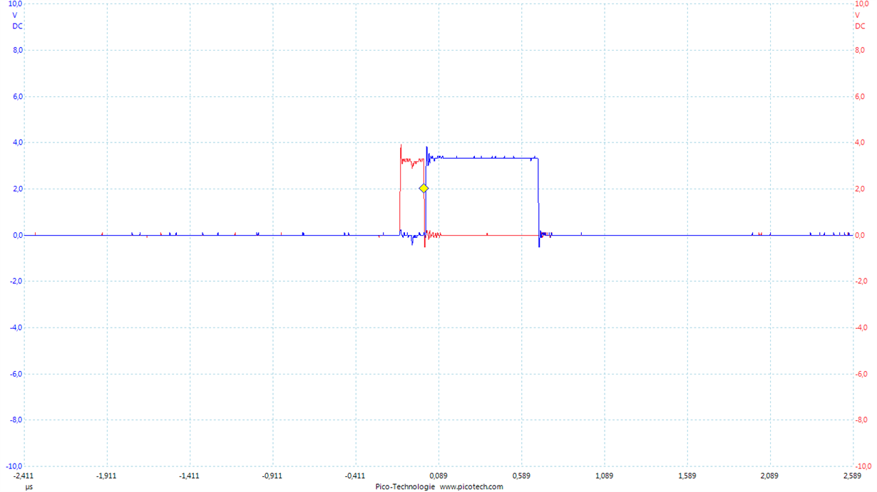
     Erroneous behaviour: Voltage level of PWM_CH (blue), PWM_CL (red) of half bridge 2.

     Erroneous behaviour: Voltage level of PWM_CH (blue), PWM_CL (red) of half bridge 2. (Zoomed)

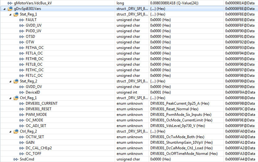
    I assume, the behaviour might be somehow related to the ability of 100% duty cycle support paired with the bootstrap circuit. However, the SPI watch window of the DRV8301 registers do not indicate any errors:

    Do you have any other ideas how to explain/fix this behaviour?

    Regards,

    Oliver

  • Oliver,

    This makes more sense. Both PWM outputs from the C28x are forced low in the fault condition, which is consistent with the TZCTL register contents in your first post. I don't know this board very well and I did not realize your first traces were measured after the DRV.

    Can you check the status of the "FAULTn" line in the erroneous condition please? That is an output from the DRV which goes into the TZ input of the C28x. It's active low, so I'm expecting it to have low pulses on it when the duty cycle is increased. If so, the DRV datasheet says it has over-currrent, over-temperature, and under-voltage protection.

    Regards,

    Richard
  • Dear Richard,

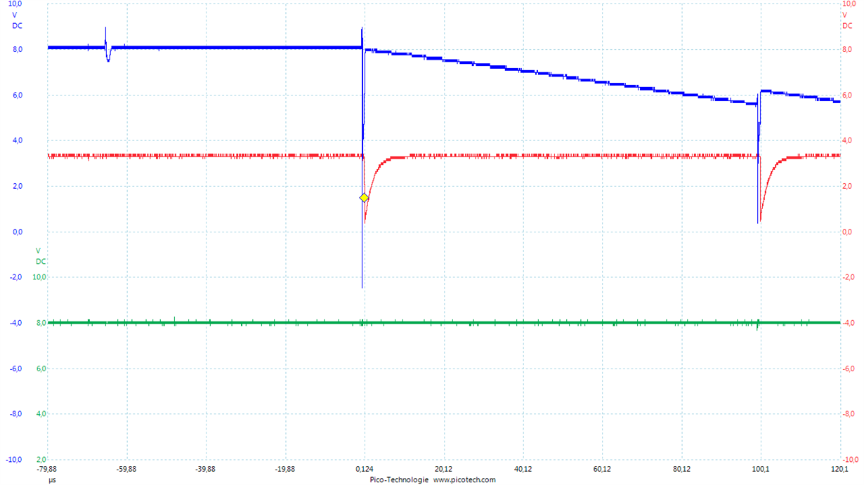
    The FAULTn line looks fine (permanently high level) but the OCTWn line indicates a warning:

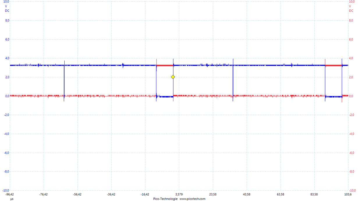
    Erroneous condition: Output voltage half bridge 2 (blue) and OCTWn signal (red)

    The OCTWn signal indicates an overcurrent or an overtemperature. In order to narrow it further down I changed the value of the variable gDrvSpi8301Vars.Ctrl_Reg_2.OCTW_SET in the SPI watch window. From the default value DRV8301_OcTwMode_Both to DRV8301_OcTwMode_OT_Only and DRV8301_OcTwMode_OC_Only. However, unexpectedly the OCTWn signal was not affected by this change. So I cannot tell you if the warning is related to an overcurrent or an overtemperature. The status registers of DRV do not indicate any errors/warnings in the watch window.

    Could the problem be related to the dead band settings of the DRV or the C28x? Is it possible that accidently both MOSFETs are switched on?

    Regards,

    Oliver

  • Oliver,

    Yes, I think so. The OCTWn line goes to GPIO13 on the '069 which is configured as a tripzone. In "hal.c:

    // OCTWn
    GPIO_setMode(obj->gpioHandle,GPIO_Number_13,GPIO_13_Mode_TZ2_NOT);

    The "GPIO_13_Mode_TZ2_NOT" indicates a TZ2 active low setting. I notice the dead-band setup in motorWARE is only 1 TB clock cycle for both rising and falling edges. In "hal.h":

    //! \brief Defines the PWM deadband falling edge delay count (system clocks)
    //!
    #define HAL_PWM_DBFED_CNT 1

    //! \brief Defines the PWM deadband rising edge delay count (system clocks)
    //!
    #define HAL_PWM_DBRED_CNT 1

    Therefore I think dead time adjustment must be handled by the DRV on this board. I see from the datasheet that dead time is an adjustable parameter on the DRV8301 chip.

    If you don't mind I'm going to move this post over to the DRV forum. I think they will be better able to help from here. If you don't get a resolution please post again on the C2000 forum and I'll pick it up. Thanks.

    Regards,

    Richard
  • Hi Oliver,

    Have you tried setting the OCP_MODE to OC latch shut down mode? This should help you isolate if it is an overcurrent event.

    If it is, please capture the VDS voltages just prior to the fault.
  • Hi Rick,

    I changed the OCP_MODE to OC latch shut down mode but the behaviour in case of an error remains exaclty the same. I recorded the voltages prior to the fault anyway:

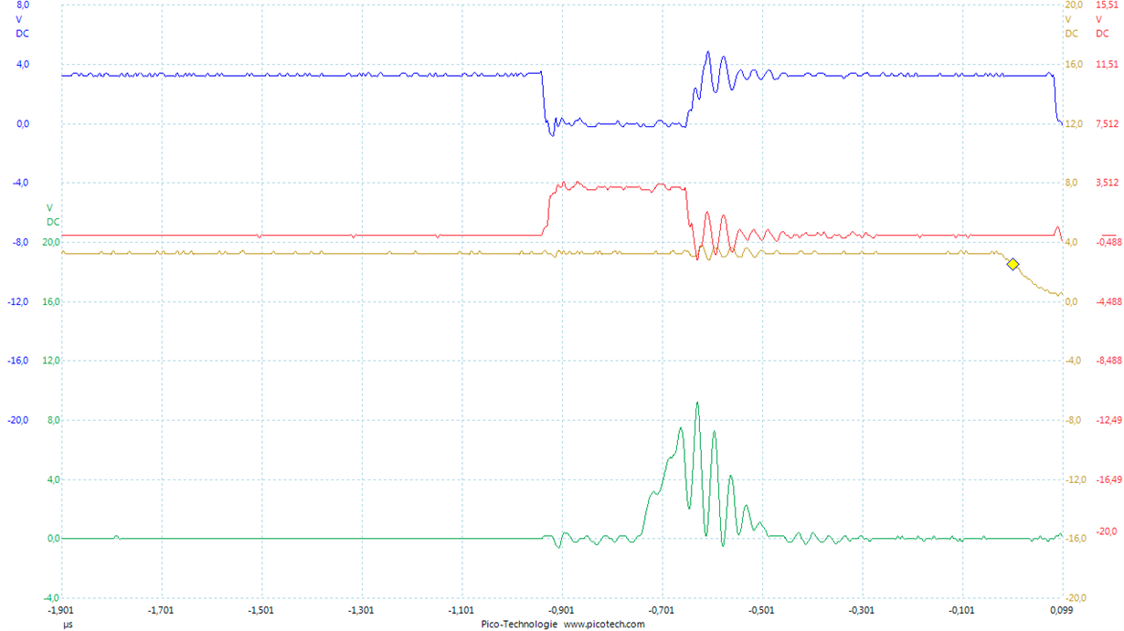
    I changed the duty cycle of half bridge 1 from -0.5 (0%) to 0.497 (99.7%) and measured the Uds voltage of the low MOSFET (blue), the DC link voltage (green) and the OCTWn line (red). Apparently, the duty cycle is adjusted properly for a couple of cycles, but then for some reason the level of the OCTWn line changes within some cycle. Here is a zoomed in view of the first fault:

    Could this be related to the bootstrap circuit?

    Regards,

    Oliver

  • Hi Oliver,

    Since the device continues to operate after the nOCTW signal asserts, this implies that it is not an overcurrent event.

    Where are you measuring the DC link voltage? If not at the DRV8301 PVDD1, can you move the probe to the DRV8301 PVDD1 pin or as close to the pin as possible? Although unlikely, voltage droops at the DRV8301 should be eliminated.
  • Hi Rick,

    Initially I measured the DC link voltage at the TP6 Terminal (DRV8301-69M-Kit). Now I rerun the procedure and measured the DC link voltage at the bulk capacitor (C7). However, the results look quite similar:

    According to the datasheet an overcurrent and/or an overtemperature are reported over the OCTWn line. What other faults can the pin indicate?

    Regards,

    Oliver

  • Hi Rick,

    is there anything else that I can test/measure to further narrow down the possible causes for this behaviour?

    Best,
    Oliver
  • Hi Oliver,

    Sorry for the delay. Is it possible to raise the voltage to 12V instead of 8V? This may help us isolate further.

    I am out of ideas at the moment but will check with others.
  • Hi Rick,

    I rerun the procedure with a DC link voltage of 12V instead of 8V and I tested another DRV8301-69M-Kit. However, the described error remains. Could the error be caused by the fact that no load is connected to the terminals?

    Kind regards,

    Oliver

  • Hi Oliver,

    Thanks for testing it at the higher voltage. It is unlikely that this is caused by an unloaded condition. Let me ping my colleagues again for their thoughts.
  • Oliver,

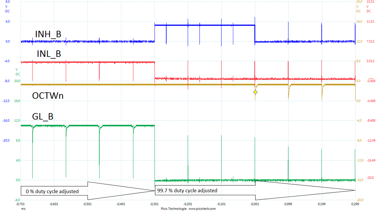
    Can you check the corresponding input signals and post here.

    It would be good to compare INHA, INLA, with OUTA to see what is happening.

  • Hi Nick,

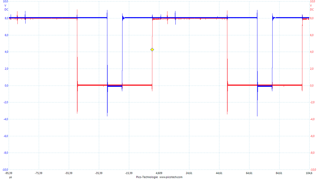
    Please find the requested signals in the measurement below.

    So to me it seems like the requested duty cycle of 99.7% can be adjusted for three cycles before the error occurs. Here is the first error on a different time scale:

    Regards,

    Oliver

  • Hi Nick,

    does this measurement give you an idea what causes this fault or do you need further information?

    Regards,

    Oliver

  • Hi Oliver,

    You need to take care at very high duty cycles.

    The gate driver uses a bootstrap architecture. Every time the half-bridge switches the bootstrap cap needs to be recharged. This enforces a minimum time in which the cap must be recharged depending on the MOSFETs used.

    The trickle charge pump supports 100% DC duty cycle when the MOSFET remain on with no switching. But when switching at high duty cycles the bootstrap cap delivers the charge.

    Example. Your control scheme could do 0 to 99% duty cycle. After 99% you need to go directly to 100%.