Other Parts Discussed in Thread: MSP430G2553,
Hello sir,
I have used DRV8305 and an MSP430G2553 controller to drive BLDC.
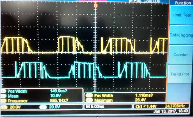
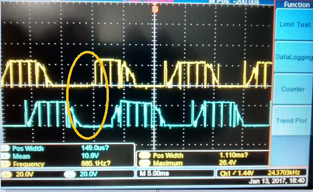
It runs almost perfectly but at some point of time BLDC motor internally make a sound for a second and that time waveform of Phase of U, V and W also get disturbed. This process is repeated but that is not at regular interval.
In my circuit, I have convert BLDC's hall sensor's 5V signal to 3.3V by using TXB0104PW. This is the image of that hall sensor circuit.

Below is code which I have taken from reference code for the one of TI reference design.
***********************************************************************************
// System Configuration
// Device Part Number	: MSP430G2553
// compiler             : Code Composer Studio 5.5.0.00077
// Oscillator Frequency	: 16MHz,  using internal DCO
// PWM generation		: TIMER A1.2, 16MHz, OUTMOD[2:0]= 2,PWM for High Side FETs
//						: TIMER A1.1, 16MHz, OUTMOD[2:0]= 6,PWM For Low side FEts
//
// Position Feedback    : Hall sensors signals
//				HA -> P2.0
//				HB -> P2.7
//				HC -> P2.6

//DRV8305
//SPI Communication		: SDO -> P1.1
//				: SDI -> P1.2
//				: SCLK -> P3.4
//				: SCS ->P3.5

//Fault Control			: EN_GATE -> P3.6
//				: FAULT ->P2.3
****************************************************************************************************/

#include <msp430.h>
#include <stdint.h>
#include "drv8305.h"

void Init_Clocks ();
void Init_IOs (void);
void Init_ADC (void);
void Init_Timer (void);
void Init_COMP_A (void);
void Hall_State_Change_FORWARD(void);
void Hall_State_Change_REVERSE(void);
void A_PWM(void);
void B_PWM(void);
void C_PWM(void);
void A_LOW(void);
void B_LOW(void);
void C_LOW(void);
void A_Z(void);
void B_Z(void);
void C_Z(void);
void Readfault(void);
#define 		PWM_PERIOD				400   //PWM Frequency (Hz) = 16MHz/((2*PWM_PERIOD)-1)
#define 		MAX_DUTYCYCLE				400   //relative to PWM_PERIOD
#define 		MIN_DUTYCYCLE				50    //relative to PWM_PERIOD
#define 		ACCEL_RATE				500   //Ramp up time to full scale duty cycle = (Full scale duty cycle) * ACCEL_RATE * PWM_PERIOD/PWM_Frequency
#define         DEAD_TIME					1     // Dead time from MSP430 = DEAD_TIME* 0.0625 uS (for 16MHz clock)
#define         Block_Rotor_Duration		             30000    //Blocked_rotor shut off time (s) = Block_Rotor_Duration*30000/Timer clock frequency
#define         WantedDutyCycle                               390     //Wanted Duty Cycle
//unsigned int DC_BUS_CURRENT = 0;
//unsigned int DC_Bus_Voltage = 0;
unsigned int SPEED_REF = 0;
//unsigned int Temperature_feedback = 0;
//unsigned int start_count =0;
volatile unsigned int HALL_STATE = 0;
volatile unsigned int softstart_counter = 0;
//unsigned int WantedDutyCycle = 390;
volatile unsigned int CurrentDutyCycle =30;
volatile unsigned int DIRECTION=0  ;
//unsigned int FirstADC_flag =1;
//unsigned int ADC_selection_flag = 1;
//unsigned int ADC_selection_flag_1 =1;
unsigned int Block_Rotor_Counter = 0;
unsigned int Block_Rotor_Counter_1 =0;
unsigned int  addr1, addr2, addr3, addr4;

/*******************************ADC channel selection*******************************************/

#define MEASURE_SPEED()		{	ADC10CTL0 = ADC10SHT_1 + ADC10IE + ADC10ON;             	\
		  	  	  	  	  	  	ADC10CTL1 = INCH_3 + CONSEQ_0 + SHS_0;						\
		  	  	  	  	  	  	ADC10AE0  = BIT3;	}
/*
#define MEASURE_TEMP()		{	ADC10CTL0 = ADC10SHT_1 + ADC10IE + ADC10ON;       			\
		  	  	  	  	  	  	ADC10CTL1 = INCH_4 + CONSEQ_0  + SHS_0;						\
		  	  	  	  	  	  	ADC10AE0  = BIT4;	}

#define MEASURE_VDC()		{   ADC10CTL0 = ADC10SHT_1 + ADC10IE + ADC10ON;             	\
		 	 	 	 	 	 	ADC10CTL1 = INCH_5 + CONSEQ_0  + SHS_0;						\
		 	 	 	 	 	 	ADC10AE0  = BIT5;	}

#define MEASURE_IDC()		{   ADC10CTL0 = ADC10SHT_1 + ADC10IE + ADC10ON;          		\
		  	  	  	  	  	  	ADC10CTL1 = INCH_6 + CONSEQ_0 + SHS_0;						\
		  	  	  	  	  	  	ADC10AE0  = BIT6;	}
*/
#define CONVERSION_ENABLE()	{   ADC10CTL0 |= ENC + ADC10SC;   }

#define CONVERSION_DISABLE() {  ADC10CTL0 &= ~ENC;								    		\
								ADC10CTL1 = 0;	   }

/*******************************Main************************************************************/
void main()
{
	WDTCTL = WDTPW + WDTHOLD;				// Stop watch-dog timer to prevent time out reset
	Init_Clocks();
	Init_IOs();
	drv8305_init();
	A_Z();
	B_Z();
	C_Z();
	if((P2IN & BIT3) == 0)
	{
		ReadRegister(0x01);
		ReadRegister(0x02);
		ReadRegister(0x03);
		ReadRegister(0x04);
		//Readfault();
	}
	P3OUT |= BIT6;
	Init_ADC();
//	Init_COMP_A ();
	Init_Timer();
	WDTCTL = WDTPW + WDTHOLD;				// Stop watch-dog timer to prevent time out reset
	__delay_cycles(1000000);
	HALL_STATE = (P2IN & BIT0) + ((P2IN & BIT6)>>4) + ((P2IN & BIT7)>>6);
	//DIRECTION =  (P3IN & BIT0);
	DIRECTION=0;
	P3OUT |= BIT1;

	while(1)
		{
			if(DIRECTION == 1)
			{
				Hall_State_Change_FORWARD();
			}
			else
			{
				Hall_State_Change_REVERSE();
			}


			if(softstart_counter == ACCEL_RATE)
			{
				softstart_counter = 0;

				if((P3IN & BIT0) == 1)
				{
					if ( CurrentDutyCycle < WantedDutyCycle )
					{
						CurrentDutyCycle++;
					}
				}
				if((P3IN & BIT0)==0)
				{
					if (CurrentDutyCycle >= 10)
					{
						CurrentDutyCycle--;
					}
				}
			}

		}
}

/**************************Initializing ADC***********************************************/
void Init_ADC(void)
{
    ADC10CTL0 = ADC10SHT_0 + ADC10ON + ADC10IE; // ADC10ON, interrupt enabled
    ADC10CTL1 = INCH_3;                         //
}

/**************************Initializing GPIOs***********************************************/
void Init_IOs (void)

{
	//Hall Sensor inputs

	P2SEL &= ~(BIT0+BIT6+BIT7);						//GPIO - Hall sensors
	P2DIR &= ~(BIT0+BIT6+BIT7);						//Inputs - Hall sensors

	//PWM outputs

	P2SEL |= (BIT1+BIT2+BIT4+BIT5);					//GPIO-PWM
	P2DIR |= (BIT1+BIT2+BIT4+BIT5);					//Output-PWM
	P3SEL |= (BIT2+BIT3);							//GPIO-PWM
	P3DIR |= (BIT2+BIT3);							//OutputPWM

	//P3SEL |= BIT7;
	//P3DIR |= BIT7;									//CAOUT

	P3SEL &= ~(BIT7);
	P3DIR |= BIT7;									//LED1


	//DRV8305
	P2SEL &= ~(BIT3);								//GPIO - FAULT
	P2DIR &= ~(BIT3);								//Inputs - FAULT
	//P3SEL |= (BIT6);								//GPIO-EN_GATE

	P3DIR |= (BIT6);								//Output - EN_GATE
//	P3OUT |= BIT6;
	//DRV8305-SPI communication
	P1DIR |= BIT7;									//GPIO-SDI
	P1OUT &= ~BIT7;									//Output-SDI
	P1DIR &= ~BIT6;									//SDO
	P3DIR |= BIT4;	//SCLK
	P3OUT &= ~BIT4;
	P3DIR |= BIT5;	//nSCS
	P3OUT |= BIT5;

	//Indications
	P3SEL &= ~ (BIT1);								//GPIO-LED3
	P3DIR |= (BIT1);								//Output-LED3

	//Direction Control
	P3SEL &= ~(BIT0);								//GPIO - DIR
	P3DIR &= ~(BIT0);								//Input - DIR

	//Enable edge interrupt for Hall sensor ports
	P2IES |= (BIT0)+(BIT6)+(BIT7);					// EDGE DETECTION   High = Falling Edge, Low = Rising Edge
	P2IFG &= (~BIT0)+(~BIT6)+(~BIT7); 				// Pin 2.0, 2.6, and 2.7 IFG cleared
	P2IE |=  (BIT0)+(BIT6)+(BIT7) ; 				// Enable Interrupt on Input Pin 2.2, 2.3, and 2.4
	__enable_interrupt();

}

/**************************Initializing Timer***********************************************/
void Init_Timer (void)
{
	TA1CCR0		= PWM_PERIOD;							// Load the Reference Count
	TA1CCTL2	= OUTMOD_2;								//High Side PWM
	TA1CCR2		= 50;
	TA1CCTL1	= OUTMOD_6;								//Low Side PWM
	TA1CCR1		= 50;									//Initialized with zero
	TA1CTL		= TASSEL_2 + MC_3 + TACLR +TAIE ;		//Up-Down Mode , SMCLK , Timer Clear; Timer Interrupt ON

	//TA1CCTL0	= CCIE;

	WDTCTL 		= WDT_MDLY_32;					// approx 2ms interval
	IE1 		|= WDTIE;                       // enable WDT interrupt
	_EINT();                              		// Enable interrupts
}

/**************************Initializing Clock***********************************************/
void Init_Clocks (void)
{
	BCSCTL1		= CALBC1_16MHZ;               	// Set DCO ~ 16 Mhz
	DCOCTL		= CALDCO_16MHZ;
	BCSCTL1 	|= DIVA_1;                    	// ACLK/(0:1,1:2,2:4,3:8)
	BCSCTL3 	|= LFXT1S_2;                  	// LFXT1 = VLO
}


/**************************Port (hall sensor) Interrupt service routine***********************************************/

#pragma vector=PORT2_VECTOR
__interrupt void    Port_2(void)

{
		HALL_STATE = (P2IN & BIT0) + ((P2IN & BIT6)>>4) + ((P2IN & BIT7)>>6);


		if(DIRECTION == 1)
		{
			Hall_State_Change_FORWARD();
		}
		else
		{
			Hall_State_Change_REVERSE();
		}


		P2IES ^= (BIT0)+(BIT6)+(BIT7);      // change the hall interrupt to falling edge to detect both the edges
		P2IFG &= (~BIT0)+(~BIT6)+(~BIT7);	// Clear Interrupt Flag

}

/**************************Timer Interrupt vector***********************************************/
#pragma vector = TIMER1_A1_VECTOR
__interrupt void TIMER1_A1_ISR (void)
{


  switch(__even_in_range(TA1IV,0x0A))
  {
  	  case  TA1IV_NONE: break;              // Vector  0:  No interrupt
      case  TA1IV_TACCR1: break;            // Vector  2:  TACCR1 CCIFG
      case TA1IV_TACCR2: break;             // Vector  4:  TACCR2 CCIFG
      case TA1IV_6: break;                  // Vector  6:  Reserved CCIFG
      case TA1IV_8: break;                  // Vector  8:  Reserved CCIFG
      case TA1IV_TAIFG:              		// Vector 10:  TAIFG


   // 	  	TA1CCR2		= (CurrentDutyCycle);
   // 		TA1CCR1		= CurrentDutyCycle;

    		TA1CCR2		= (CurrentDutyCycle -DEAD_TIME );
    		TA1CCR1		= CurrentDutyCycle;

    		if((P2IN & BIT3) == 0)
    		{
    			P3OUT &= ~(BIT6);
    			Readfault();
    		}


      break;


      default: 	break;
  }
}


/**************************ADC INTERRUPT***********************************************/
#pragma vector=ADC10_VECTOR
__interrupt void ADC10_ISR (void)
{


	 SPEED_REF = (ADC10MEM>>1);
	 CONVERSION_DISABLE();

  }

/**************************Commutation sequence Forward***********************************************/
void Hall_State_Change_FORWARD(void)
{

			switch (HALL_STATE)
			{
				case 2:
						A_PWM();
						B_LOW();
						C_Z();

				break;

				case 6:
						A_PWM();
						C_LOW();
						B_Z();

					break;

				case 3:
						C_PWM();
						B_LOW();
						A_Z();

						break;
				case 1:
						C_PWM();
						A_LOW();
						B_Z();

						break;

				case 4:
						B_PWM();
						C_LOW();
						A_Z();

						break;

				case 5:
						B_PWM();
						A_LOW();
						C_Z();

						break;


				default:
					A_Z();
					B_Z();
					C_Z();

					break;
			}


}
/**************************Commutation sequence Reverse***********************************************/
void Hall_State_Change_REVERSE(void)
{

			switch (HALL_STATE)
			{
				case 2:
						B_PWM();
						A_LOW();
						C_Z();

				break;

				case 6:
						C_PWM();
						A_LOW();
						B_Z();

					break;

				case 3:
						B_PWM();
						C_LOW();
						A_Z();

						break;
				case 1:
						A_PWM();
						C_LOW();
						B_Z();

						break;

				case 4:
						C_PWM();
						B_LOW();
						A_Z();

						break;

				case 5:
						A_PWM();
						B_LOW();
						C_Z();

						break;


				default:
					A_Z();
					B_Z();
					C_Z();

					break;
			}


}

/**************************Definition of PWM GPIOs***********************************************/

void A_PWM(void)

{
	P3SEL |= BIT3;
	P3SEL |= BIT2;

}


void B_PWM(void)

{
	P2SEL |= BIT4;
	P2SEL |= BIT2;

}

void C_PWM(void)

{
	P2SEL |= BIT5;
	P2SEL |= BIT1;

}

void A_LOW(void)
{
	P3SEL &= ~BIT3;
	P3OUT &= ~BIT3;
	P3SEL &= ~BIT2;
	P3OUT |= BIT2;
}

void B_LOW(void)
{
	P2SEL &= ~BIT4;
	P2OUT &= ~BIT4;
	P2SEL &= ~BIT2;
	P2OUT |= BIT2;
}

void C_LOW(void)
{
	P2SEL &= ~BIT5;
	P2OUT &= ~BIT5;
	P2SEL &= ~BIT1;
	P2OUT |= BIT1;
}

void A_Z(void)
{
	P3SEL &= ~BIT3;
	P3OUT &= ~BIT3;
	P3SEL &= ~BIT2;
	P3OUT &= ~BIT2;
}

void B_Z(void)
{
	P2SEL &= ~BIT4;
	P2OUT &= ~BIT4;
	P2SEL &= ~BIT2;
	P2OUT &= ~BIT2;
}

void C_Z(void)
{
	P2SEL &= ~BIT5;
	P2OUT &= ~BIT5;
	P2SEL &= ~BIT1;
	P2OUT &= ~BIT1;
}

void Readfault(void)
{

	addr1 = ReadRegister(0x01);
	addr2 = ReadRegister(0x02);
	addr3 = ReadRegister(0x03);
	addr4 = ReadRegister(0x04);

}
/**************************End****************************************************************/
So please help me for this. You can point out a error in code also.
Thank you.
Best Regards,
DINESH JINJALA