This thread has been locked.

If you have a related question, please click the "Ask a related question" button in the top right corner. The newly created question will be automatically linked to this question.

DRV595: FAULTZ pin behaviour

Part Number: DRV595

Hi whomever it concerns!

Regarding the FaultZ pin.

In application it is pulled up to 3.3V with 100k

In application I have pulled the SDZ low.

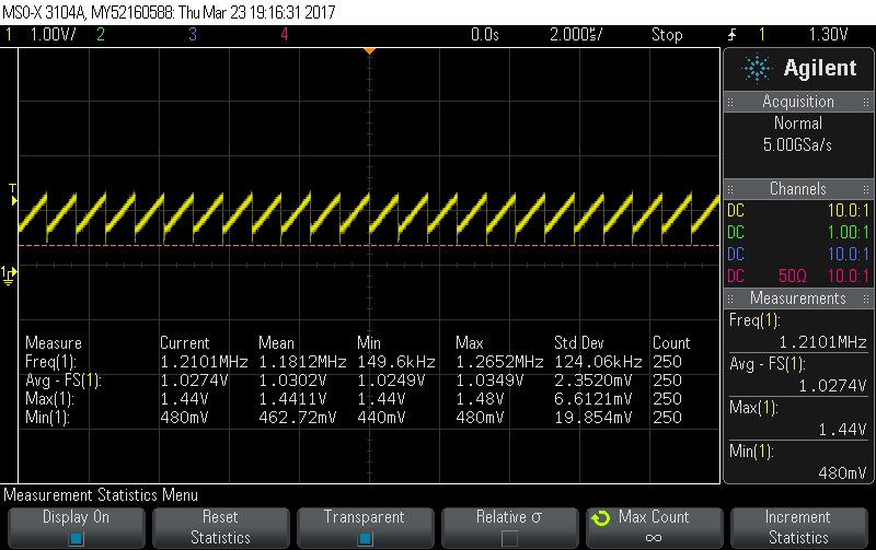
Attached the behaviour of the Faultz pin at 4A on the device.

It is not compltely clear to me how to calculate the pull-up at other supply voltage than the 26V. You refer to 26V in the datasheet.

I expected a distinct on/off when a failure due to overcurrent or to high temperature on the device.

Could you please advice?

  • Hello Anders,
    Our experts have been notified and should reply soon.
    Thank you.
  • Id itHi Anders,

    Thanks for asking question in E2E. For FAULT pin, a pull-up resistor is recommended to limit the slew rate of the voltage which is presented to the pin during power up. Depending on the output impedance of the supply, and the capacitance connected to the power net on the board, slew rates of this node could be high enough to trigger the integrated ESD protection circuitry at high current levels, causing damage to the device. 100kOhm is recommended to be used here. I think you could use a little lower value resistance for a lower level power supply. 

    About the FAULT pin waveform shown in the picture, is it triggered by over-current protect?  Not DC protect or OT protect? If it is OC protect, could you please also capture the output curent waveform on the scope? Could you please let me know the load on the output?

  • Hi Shawn! Thanks for your prompt reply. The current is 4A when the trace is captured. The device is as I can understand operating as It should. I have a DC output. Output is about 7V and power suppy is 24V so the duty should be ok. As I can see It seams to be temperature related. Increasing the current will lower the average voltage on the faultz pin and finally the device shuts off. I really do not get the output behavior. Best regards Anders
  • Hi Anders,
    From the above captured screen, the FAULT voltage ranges from 0.44V to 1.48V, with being pulled up to 3.3V through 100kohm resistance. This waveform is strange. During this measurement, FAULT seems being clear by SDZ. So could you please provide your SCH?
    Best regards,
    Shawn Zheng
  • Only a pull-up to 3.3V on FaultZ and then directly to the MCU.

    SDZ is driven high and there is a resistor 100k to GND.

    Hi-Z is driven low with both 100k pull-up and pull down.

    However I noticed that I am running the device at the reserved setting FS2=1, FS1=1 and FS0=1

    Could this be a reson for the strange behaviour?

    The ripple I see point at FS2=1, FS1=0, FS0=0

    I will look at the board more in detail if there is any remaining solder bridges.

     When the device is not loaded hard the faultZ average value is higher and the ripple is lower than in previous picture.

    Supply voltage only drops from 23.6V down to 23.2V during loading.

    When increasing the current to 4.4A the signal  average drops,   average 92mV with ripple 900mV at 1.2Mhz and signals is locked in this level and output to the load is shut-off.

    Is this a reserved mode so that can be used for monitoring the chip temperature?

  • Hi Anders,

    As you said, the reserved setting for FS0~FS2 can't be used in the application.

    In previouos waveforms shown above, the ripple on the FAULTZ pin has 1.2MHz frequency, which is the samae as FS setting, so I think it should be related to the PWM switching. I think you need to check the EMI and the signal integration on your board, or solder and grounding on the board. 

    About the chip temperature, the device has thermal protect - the device gets into shuntdown mode if the internal die temperature exceeds 150°C+/-15°C.

    Best regards,

    Shawn Zheng