This thread has been locked.

If you have a related question, please click the "Ask a related question" button in the top right corner. The newly created question will be automatically linked to this question.

DRV8323R: About the signal abnormality of DRV8323

Part Number: DRV8323R
Other Parts Discussed in Thread: CSD88584Q5DC, DRV8323, CSD88599Q5DC

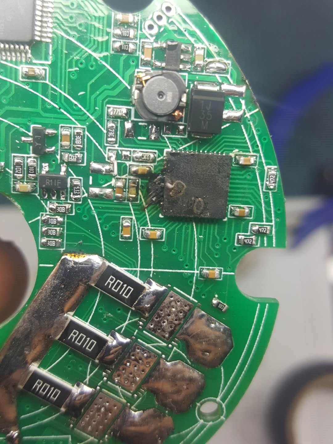
My motor driver is implemented using the DRV8323RX+CSD88584Q5DC

In the application, a mismatch between the gate drive signal and the PWM signal is encountered, causing the motor to start desynchronizing.
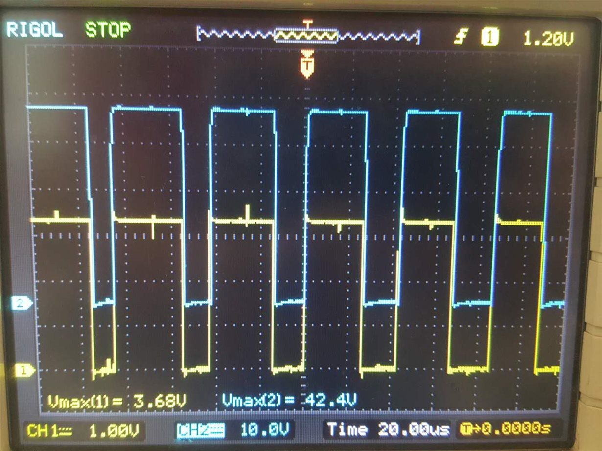
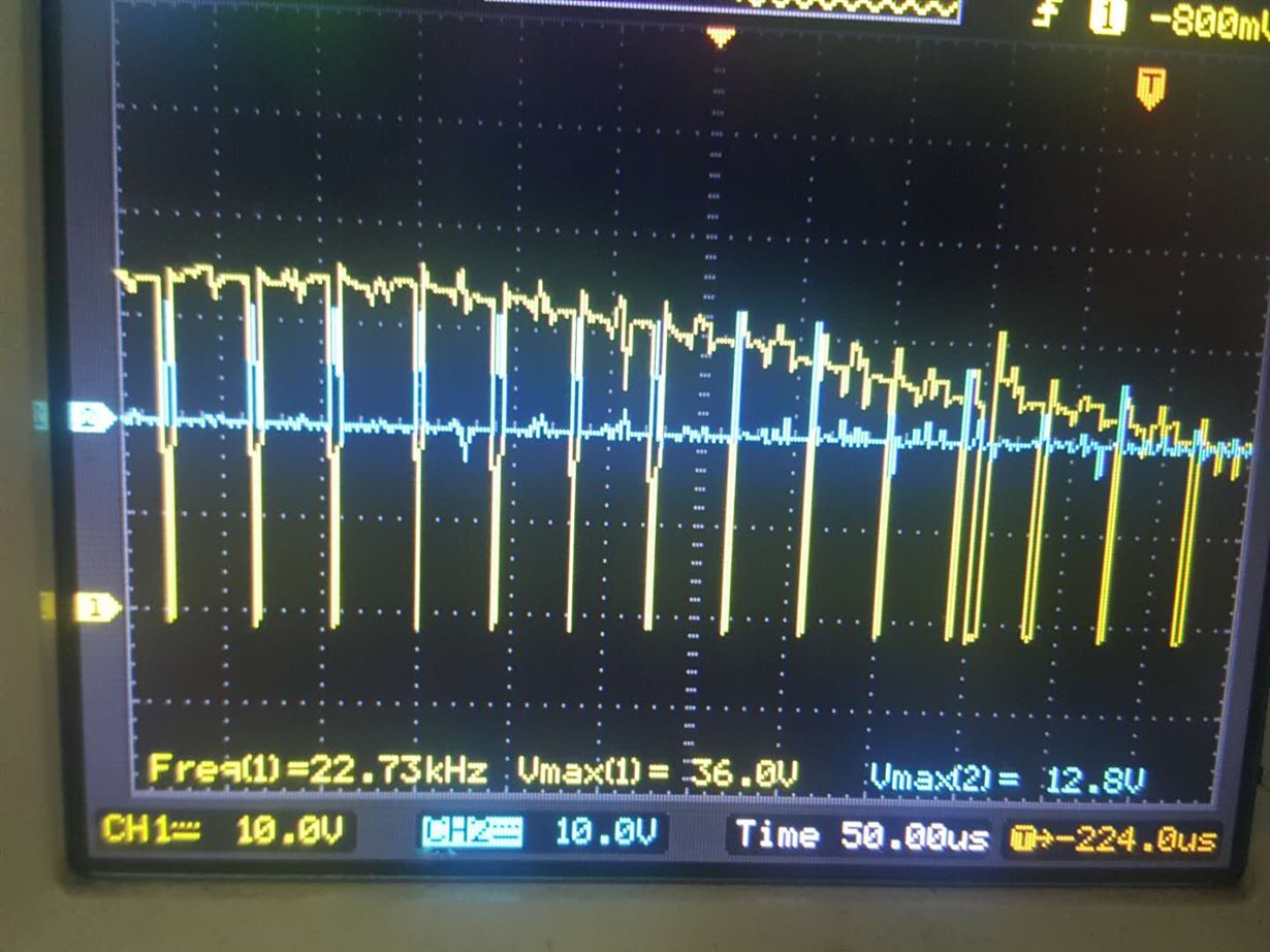
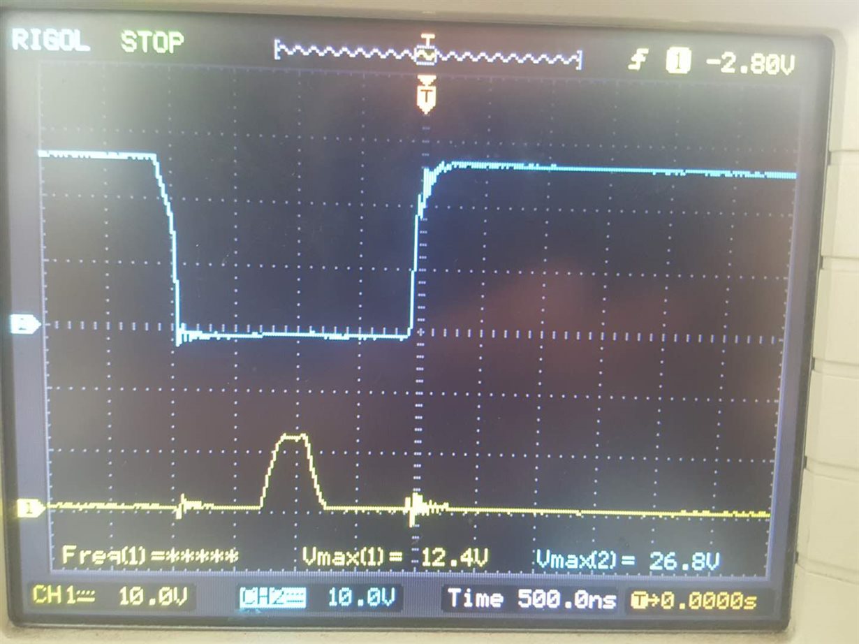
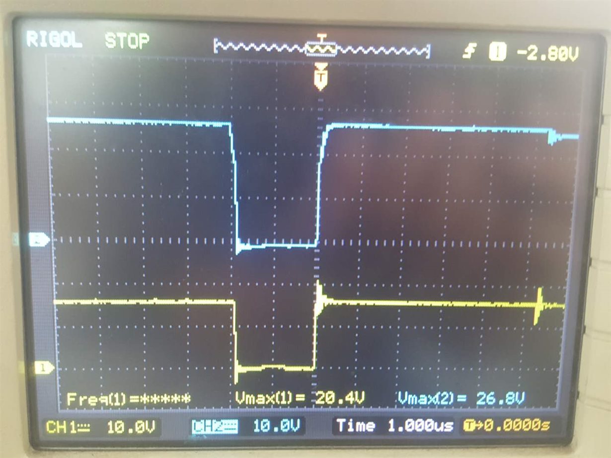
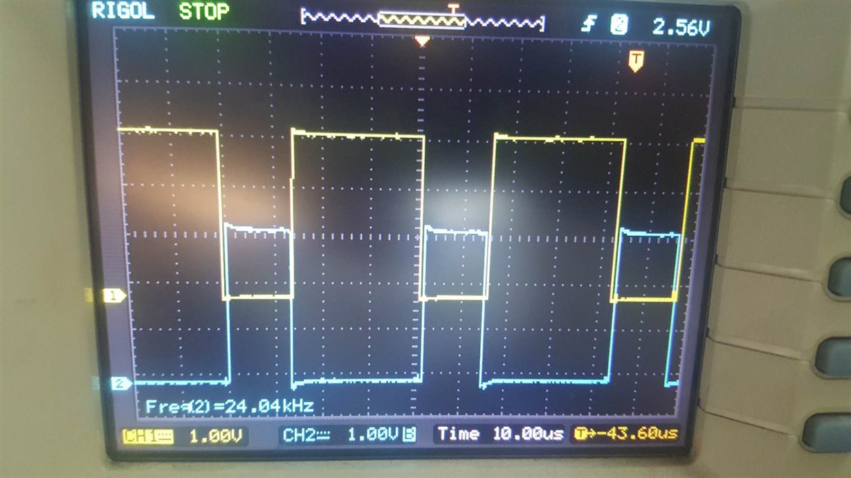
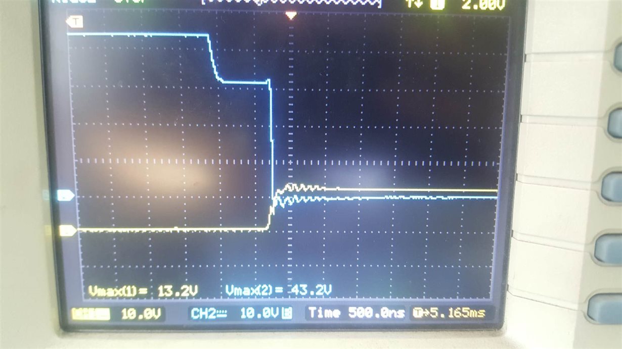
The waveforms measured using a normal MOS driver IC are as follows: (CH1pwm waveform, CH2 drive waveform)

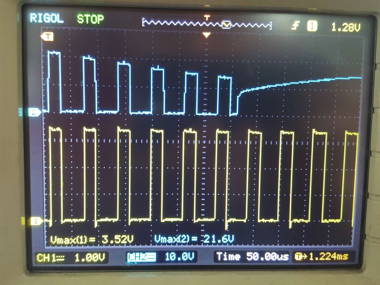
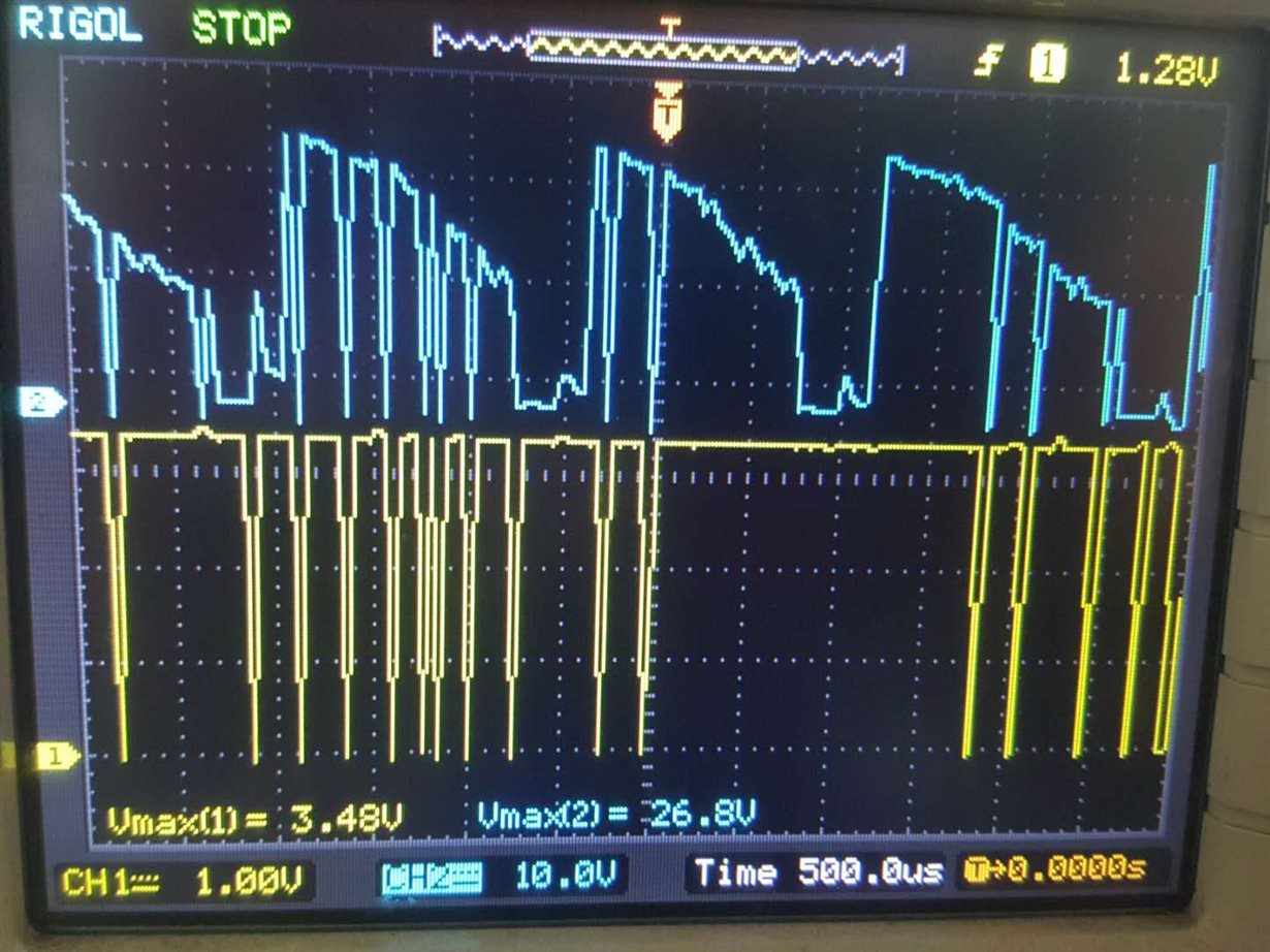
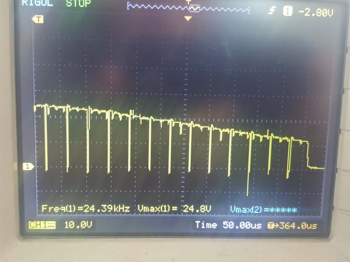
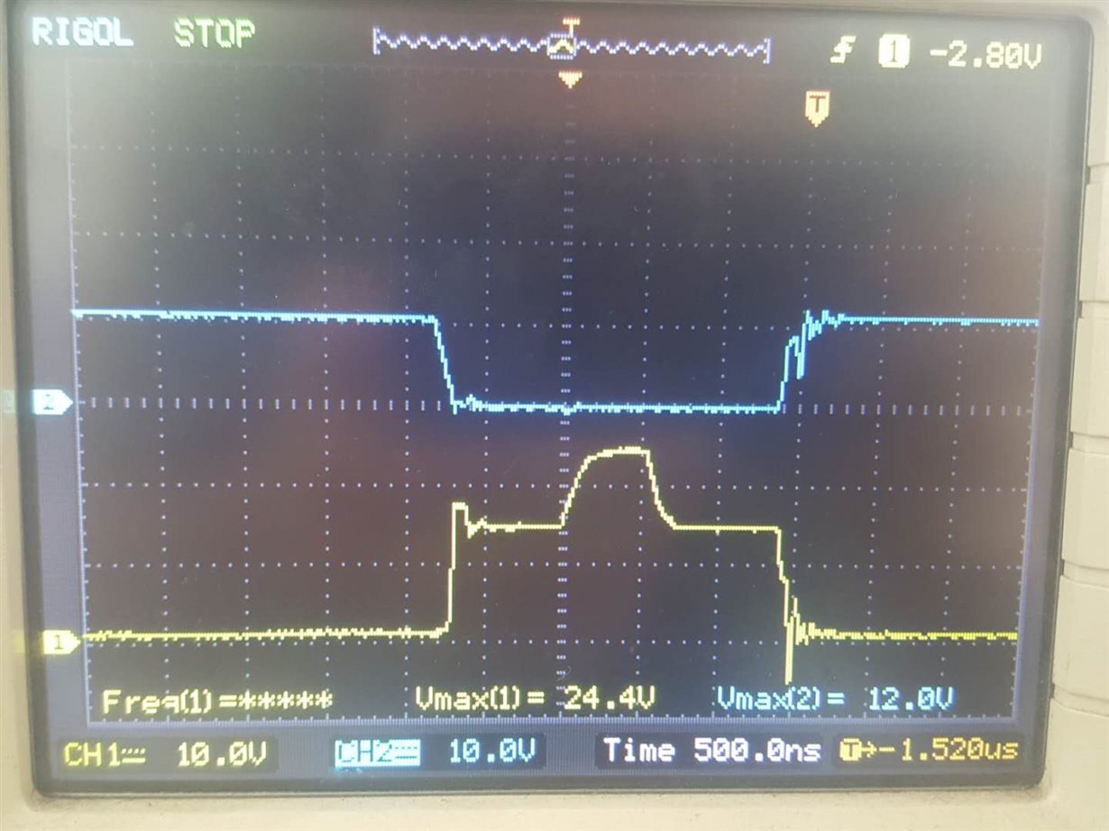
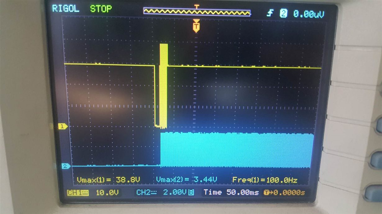
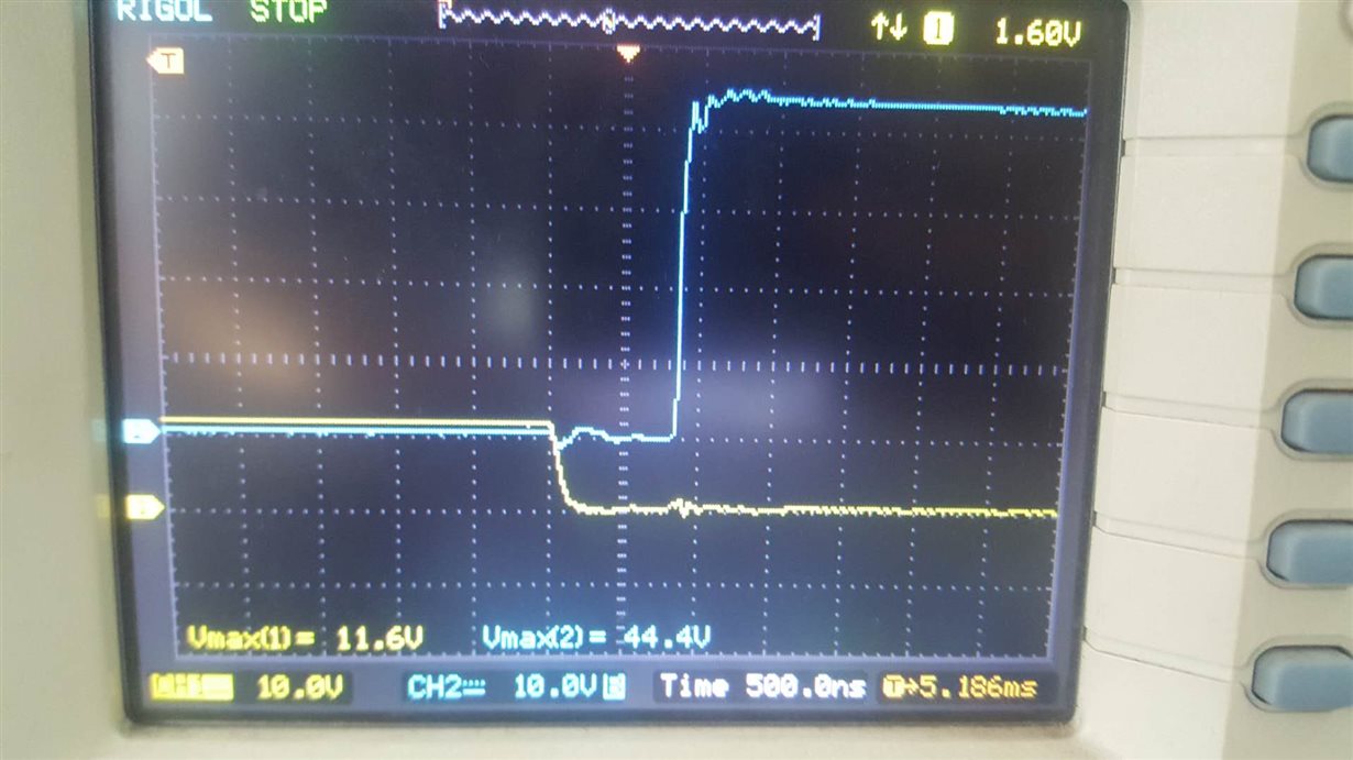
Then measure the output waveform and PWM waveform of the DRV8323RX:

The settings for the DRV8323RX in the program are:

SPI_ReadWriteByte(0x1000);
SPI_ReadWriteByte(0x1BFF);
SPI_ReadWriteByte(0x27FF);
SPI_ReadWriteByte(0x2D59);
SPI_ReadWriteByte(0x3203);

What is the reason for the abnormality of the drive signal? I never found the reason.

  • Hi Yingzhi,

    Can you provide more information about your question.
    1. what's the normal MOS drive IC in first figure?
    2. how about the VM and nFAULT waveform of DRV8323?
    3. what's the load current?

    Thanks.
  • Hi Betty,

    1,The first figure of the normal MOS drive IC is L6389,from ST.

    2,When i go to try to start the motor. After one rotation of the motor,nFAULT go to LOW. SO i read the value of the register,Fault Status 1 and VGS status2.Every time the fault is the same:Indicates gate drive fault condition, sometime is HA fault,sometime is HB fault,sometime is HC fault.    Last night ,I changed the register:Gate drive fault is disabled,and start the motor.oh~motor is running. But After 10 seconds,DRV8323RS exploded..so bad.

    3,The start current is 500ms 4A,1000ms 8A,1500ms 10A,  if the motor is running,load current is 2A.

  • Yesterday, I set TDRIVE is 4000ns, CSD88599Q5DC's Qgd is 7nC,and tr 100ns, so I set IDRIVEP and IDRIVEN is 120ma. is it right?
    and CSD88599Q5DC's 56nC,and Ivcp > 3*Qg*Fpwm. so I set Fpwm is 24KHZ. 3*56nC*24K=4.032ma<25ma.

    thand you so much.
  • Hi Betty,

    I made a new PCB,The old one is exploded.

    But the same situaion. The GHX and GLX will fall.

    This GHA and SLA,

    I tried all Idrive and Tdrive settings,Idrive form 0x00 to 0xff.Tdrive is from 500ns to 4000ns.But same.

  • Hi Yingzhi,

    1. I checked the CSD88599Q5DC datasheet, the tr=20ns, Qgd is 7nC, so IDRIVEP should be 350mA. The PWM frequency is 24k, it is ok.
    2. Strong recommend that DONT disable Vgs fault detection.
    3. As your description, the problem maybe is Vgs control.Can your show me the circuit between GHX,GLX and CSD88599Q5DC gate ? is there any resistors? Because the resistor will effect the MOSFET switch time.
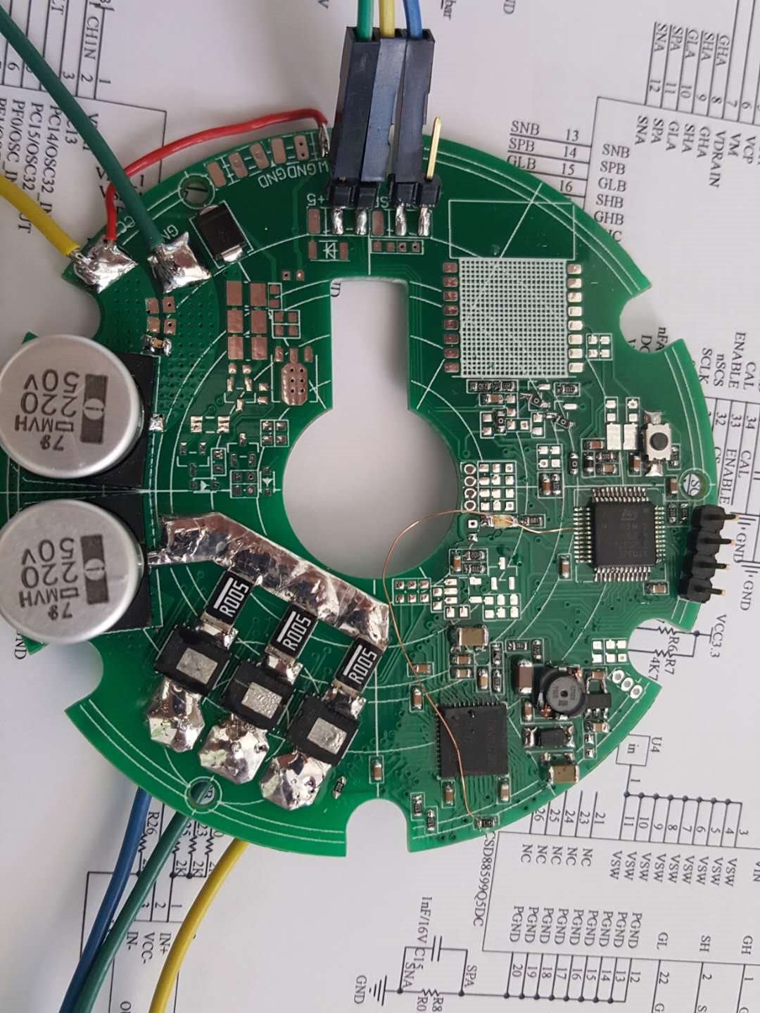
    4. I find six 30B resistors on your PCB board, what are they used for?

    Thanks.
  • Hi,Betty,

    I uploaded my schematic .

    3.No resistor connected between GHX,GLX and CSD88599Q5DC.

    4.These resistors are used for BKIN detection.

    thank you so much.

    Schematic Prints.pdf

  • Hi Betty,

    This is my new PCB. I removed some unrelated to the operation of the motor.But the same situation.

  • Hi Yingzhi,

    A bulk capacitor must be included on VM pin, the value should be depend on your application. please see DRV8323 datasheet P69 about bulk capacitor section. I found you only placed a 4.7uF/50V capacitor on VM, it too small.

    if your still have questions, please let me know.

    Thanks.
  • Hi Betty,

    I changed these parameters.

    IDRIVEP:370ma  IDRIVEN:380ma     TDRIVE:2000ns  VDS_LVL:0.75V  SHUNT R:0.005Ω

    And try to start the motor,nFAULT go to Low. The Fault Status Register1 is VDS_HA, or VDS_HB.

    I changed the capacitance 47uf on VM.  The fault is the same.Indicates VDS overcurrent fault on the high-side MOSFET.

    and GHA waveform is this:

  • Hi Yingzhi,

    please measure the high side Vgs signal , Low side Vgs signal and deadtime.

    CSD88599Q5DC fall time is 2ns, so change the IDRIVEN to max, and measure how long the MOSFET need to turn off.

    Thanks.
  • Hi Betty,

    I measured the signal about GHA and GLA at startup.

    Then also signals of GHA and MOTA.

    When the motor startup.Power start to go low.My power is 30V15A.

  • Hi Betty,

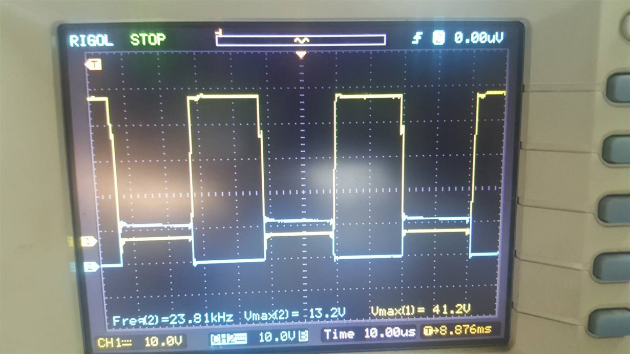
    I think I see an abnormal situation.  This is an incorrect waveform.GHB and GLB.

    The waveform is weird. And deadtime disappeared.  This wavefrom does not happen every moment.

    Then I went to measure INHB and INLB.

     This is INHB and INLB wavefrom.

  • Hi Betty,

    DRV8323RS input logic high voltage is 1.5V. I thank it is the problem of the jitter of the input signal waveform of INHX and INLX.
    So I plan to change the PCB, Add to Res-Cap Circuits between MUC and INHX,INLX . Do you think this is feasible?
  • Hi Yingzhi,

    A better way is to change PCB layout to reduce this jitter. Usually there is not need RC circuit between MCU and DRV, because you can control the  MOSFET switch time by Idrive.

    Thanks.

  • Hi Betty,

    I changed my PCB this week.Now INHX and INLX signals are perfact:

    But there are the same problems as before:Indicates gate drive fault on the X high-side MOSFET,20ms after start motor is FAULT.I tried to modify Idrive and Tdrive again.But failed.

    I measured the waveforms of GHX and INHX :

    Now the gate drive voltage will not fall.

    I measure the high side Vg signal and LOW sige Vg signal.

    The deadtime does not seem normal.

    I have no idea, What should I do next?

    thank you so much.Please forgive my stupidity.

    180518FOC_Project.rar

  • Hi Betty,

    I tried to start the motor several times. DRV8323 is broken. VM,VCP,VPH,BGND,AGND,DGND is connected.
    1uf/50V between VM and VCP,47nf/100V between CPH and CPL.
    I do not know why .

    Thank you for you help.
  • Hi Yingzhi,

    input signals looks ok.

    please zoom in your last picture to measure dead time and what's the Idrive in this picture?

    I see the high side Vg signal and low side Vg signal have overshoot. base on datasheet, the GHX range is -5V to VCP+0.5 and GLX voltage is -0.5V to 13.5V, so please check your signal voltage, maybe it the reason of device damage.

    also, what's the gate signal of high side and low side when devices damage?

    thanks.
  • Hi Betty,

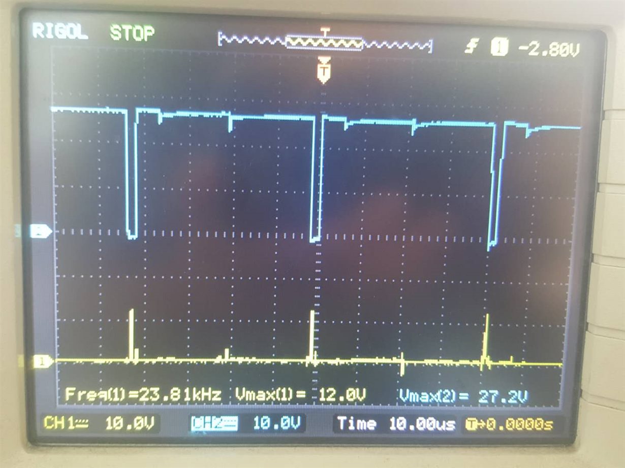
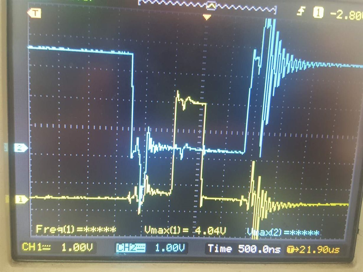
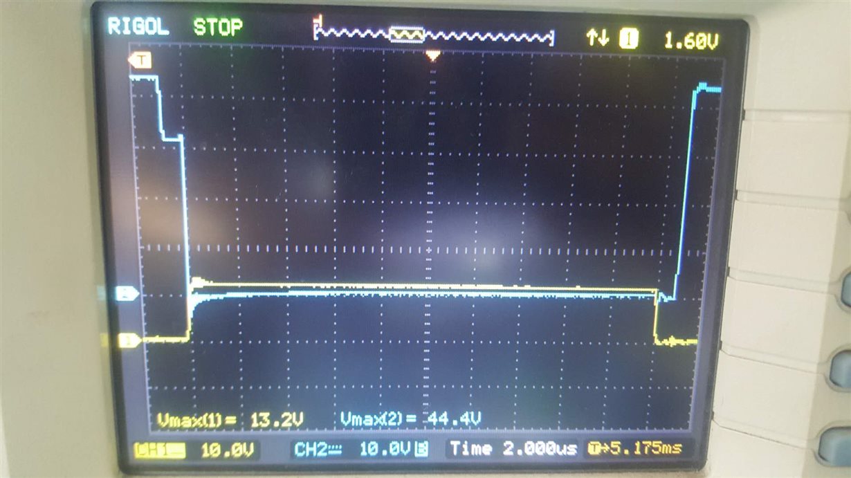
    I zoomed in on the picture:

    The IDRIVEP is 680ma,IDRIVEN is 740ma,  TDRIVE is 4000ns.DEAD_TIME is 100ns.

    And the dead time in my software is 800ns.

    DRV8323RS is not damaged again.So I did not capture the signal.

    Also, Internal LMR16006X in DRV8323, The DC-DC efficiency is very low. Is this related to the driver?

  • Hi Yingzhi,

    dead time looks ok. Does the device working normally?

    Internal dc/dc is work independently, you can refer to datasheet.

    thanks.
  • Hi Betty,

    My controller still doesn't work. I will check my software. But i don't have a good idea.Because my software is normal on other PCBs.

    thanks.