This thread has been locked.

If you have a related question, please click the "Ask a related question" button in the top right corner. The newly created question will be automatically linked to this question.

DRV8703-Q1: SPI Communication problems

Part Number: DRV8703-Q1

I am trying to SPI communicate to DRV8703-Q1 and I use following arduino SPI code:

void testSpi()
{
  usleep(10);
  // SPI WRITE
  vspi->beginTransaction(SPISettings(spiClk, MSBFIRST, SPI_MODE0));
  //byte stuff = 0b11001100;
  //hspi->transfer(stuff);
  digitalWrite(SS1, LOW);
  toTransfer = 0b11001100 << 8;
  toTransfer |= 0b11001100 ;
  vspi->transfer16(toTransfer);
  digitalWrite(SS1, HIGH);
  vspi->endTransaction();
  usleep(10);
}

I dont get any reply from device.

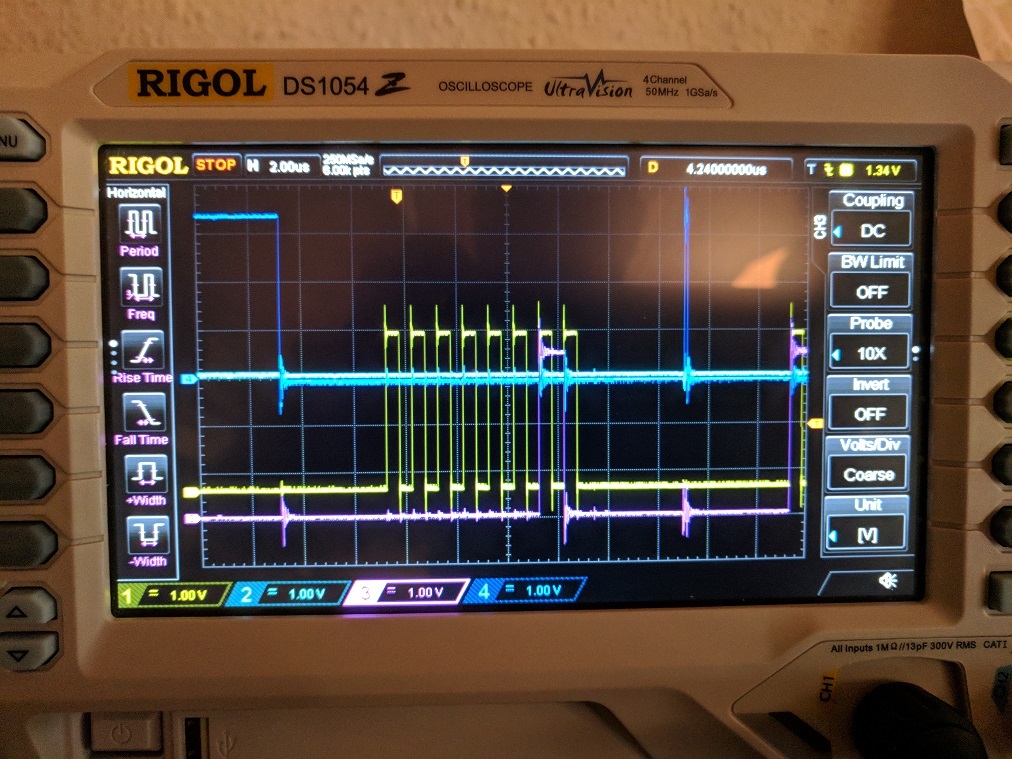
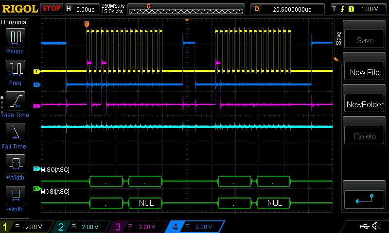
Picture of SPI Communication is attached -

channel1 - yellow : CLK

channel2 - light blue: SS (Slave select)

channel3 - pink: MOSI

channel4 - dark blue: MISO

Wht could be the problem? Any idea how to troubleshoot further?

regards

  • Hi Zhivko,

    Please note from section 7.5.1.1 of the datasheet:

    Data is captured on the falling edge of the clock and data is driven on the rising edge of the clock.

    It appears the data is driven on the falling edge in your scope capture.

    Also, a good practice in debugging SPI transactions is to read a register with known non-zero data (Address 0x02 reads 0x18 on power up). If you can read this, the SPI should then be operational.
  • Hi Rick,

    I corected SW, and now MOSI is on falling edge of SCL.

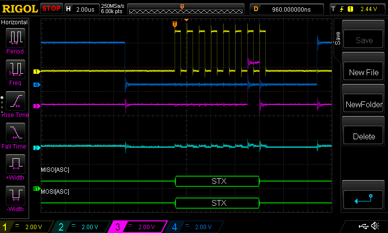
    Still no reply from chip - see picture of scope trace (yellow scl, pink MOSI).

    Do you maybe know what is max SPI CLK Speed in MHz ?

  • Hi Zhivko,

    There are a few items to check:
    1) Is nSCS toggling high then low after 8 clocks? If yes, please change the sequence to avoid nSCS toggling between each 8 bits.
    2) Do you have a pullup resistor on SDO? Without a pullup, there is no valid data.
    3) If you do have a pullup resistor, what is the value? A pullup of approximately 3k should be sufficient.
    4) Which address are you trying to read? It appears like address 0x0, but you should try 0x2, 0x3, 0x4, or 0x5 because these are non-zero.

    If you still need assistance, would you please change the scale/position of the channels? There are a few channels that are overlapping, making it difficult to interpret. Thank you.
  • Hi,

    here are answers:

    1) Is nSCS toggling high then low after 8 clocks? If yes, please change the sequence to avoid nSCS toggling between each 8 bits.

    Ok disabled it now although I am not sure why this would help. Nothing better... Still no reply.


    2) Do you have a pullup resistor on SDO? Without a pullup, there is no valid data.

    No I dont have resistor - where in datasheet is this mentioned? Also schematics images are without pullup on SDO in datasheet - why?


    3) If you do have a pullup resistor, what is the value? A pullup of approximately 3k should be sufficient.

    No pullup now.


    4) Which address are you trying to read? It appears like address 0x0, but you should try 0x2, 0x3, 0x4, or 0x5 because these are non-zero.

    I am trying to read 0x02.

    Please see more clear picture adapted as you suggested (previous was taken with phone).

    regards

  • Hi Zhivko,

    Thank you for the updated scope capture.

    1) Pullup requirement is stated in the Pin Functions Description for SDO. "This pin is an open-drain output that requires an external pullup resistor." Please add the pullup. This can be done either externally or by enabling a pullup if the mcu has it available. The mcu pullup may not allow maximum SPI speed.

    2) Can you confirm channel 4 is nSCS, channel 1 is SCLK, and channel 3 is SDI? Is this is correct, you are trying to perform a read of address 0. Please read section 7.5.1 (SPI Communication) for the conditions of a valid frame.
    You need 16 clocks to perform a valid transaction
    nSCS should be low during the entire 16 clock sequence
  • Hi Rick!

    regarding 1 - OK found it now...

    regarding 2 - yes you got channels correctly

    Seems I need to persuade arduino to make 16 cycles SCLK of SPI transaction somehow.

    Currently my code is:

     vspi->setDataMode(SPI_MODE2);

     vspi->setHwCs(false);

     usleep(1);

     digitalWrite(SS1, LOW);

     // SPI WRITE

     vspi->beginTransaction(SPISettings(spiClk, MSBFIRST, SPI_MODE2));

     uint8_t reply = vspi->transfer(0x02);  // should return 0x18

     vspi->endTransaction();

     digitalWrite(SS1, HIGH);

     usleep(1);

     Serial.println(reply);

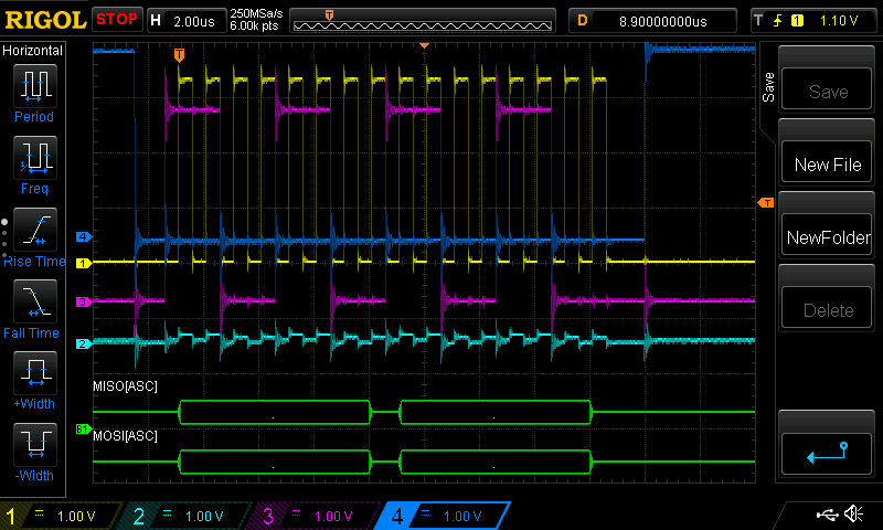
    And scope traces with pullup on SDO is:

    Sorry but isnt thi's 02x on MOSI line - second down on clk crossed with mosi line? 02x = 0010 binary - no ?

  • Hi Zhivko,

    "Sorry but isnt thi's 02x on MOSI line - second down on clk crossed with mosi line? 02x = 0010 binary - no ?"

    No it is not. The 8 bits from left to right should be 00010xxx. Please note Table 12 and 13 for the information.

    Once you fix the data on the MOSI line and keep nSCS low during the entire 16 bits, you should be able to read data from register 0x2.
  • According to this:

    SPI mode Clock polarity
    (CPOL/CKP) Clock phase
    (CPHA) Clock edge
    (CKE/NCPHA)
    0 0 0 1
    1 0 1 0
    2 1 0 1
    3 1 1 0

    What SPI mode should I use?
  • Hi Zhivko,

    Your settings appear to be correct. The data sent does not appear to be correct. For a read of address 2, the 8 bits should be 00010xxx in the scope capture.
  • Hi RIck,

    sorry but it seems I have problem preparing data for MOSI line to be sent.

    Now I am trying 02x address as you see from picture:

    1 is READ than I have

    10010 Is READ from addres 2 (02x). I still dont get any reply - please see scope trace of first 16 CLK (two bytes) - next 16CLK is read of fault address:

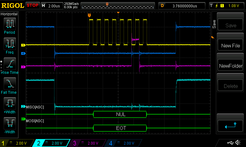
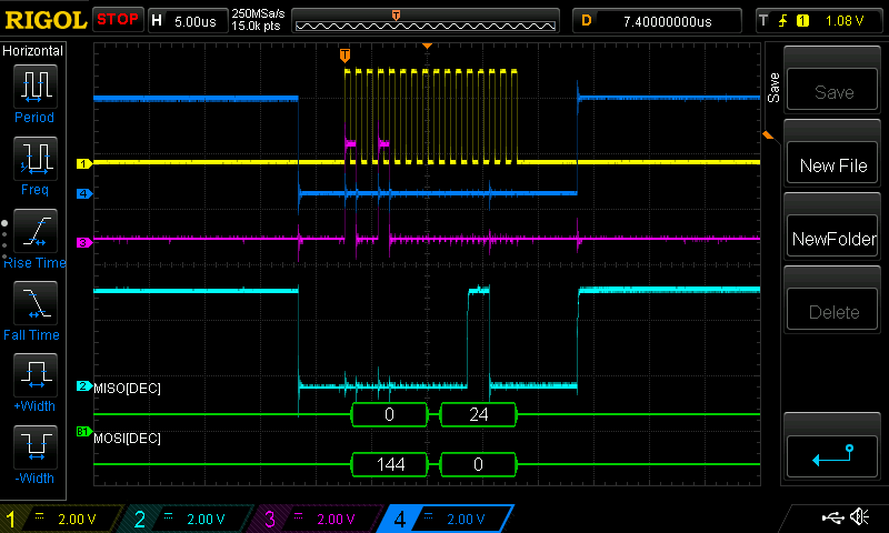
  • So acording to my calculation (please correct me if I m wrong) read from addres 02x is 10010000 binaray or 144 decimal - and as you can see RIGOL also shows 144 decimal on MOSI line:

    Also I think that "Data is captured on the falling edge of the clock and data is driven on the rising edge of the clock." is OK since MOSI is forcing data on CLK down edge - so why there is no reply from  is wrong ?

    .... sorry - after turning on VM - 12V, I finaly got something back on MISO line:

  • Hi Zhivko,

    Glad to see you have it working. And you are correct; a read of address 2 should be 10010000.