This thread has been locked.

If you have a related question, please click the "Ask a related question" button in the top right corner. The newly created question will be automatically linked to this question.

PMP9477: Automotive Start-Stop Reference Design Demo

Part Number: PMP9477
Other Parts Discussed in Thread: LM3481, TIDA-00744, TPS55340

Hi,

I have noticed some discrepancies in this video regarding what Mr. Xiang was telling and what he had showed.

Video Link: https://www.youtube.com/watch?v=78UR5jJQj4Y 

  1. Video time 5:35: He was explaining that the Boost Converter is in bypassing mode but according the schematic PMP9477 Rev. 3 this circuitry for bypassing mode is not populated. This can be also noticed at Video time 2:58 where U4 is not populated. Could someone explain how the LM3481 will be setup in the bypass mode? 
    On the other Hand, a reference design  TIDA-00744  Rev. E1 have the bypassing circuit with transistor Q1. This circuit can not be found in PMP9477 schematic. Could you explain why?
      
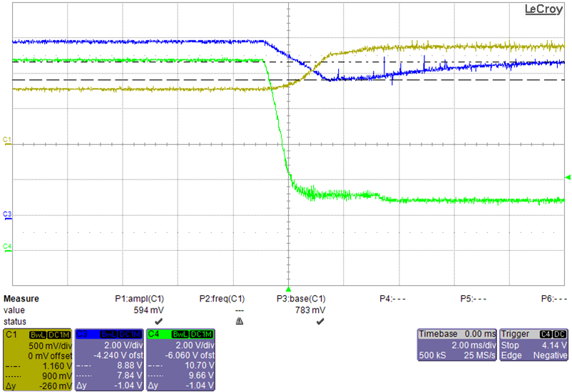
  2. Video time 5:18: He said 2V/Div and 12V Input, but from my point of view it looks like  11V. Is that correct?

  3. Video Time 5:50: If the Channel 1 (VIN) and Channel 2 (VMID ...Boost output) have the same reference 0V Position, then the VMID will be 8V. Correct?  
    Why the PMP9477 Rev. 3 Schematic states 9.5V 1.5A?

    I am quite confused regarding  this presentation.

Best regards,

Josko

Hi,

I have noticed some discrepancies in this video regarding what Mr. Xiang was telling and what he had showed.

  • Additional question:

    How was achieved constant running of LM3481 for voltages above 9V? Is the LM3481 switching going on above 9V? If the LM3481 is bypassed for voltages above 9V, how was possible to have so quick Line Response for the LM3481? I mean on the input voltage change from 12V downwards to the 4.5V.
    If it is possible, I would like to have diagram with 500uS/Div trigger on the falling edge at the momnet when Input voltage make the change from 12V downwards to 4.5 V. Thanks in advanced.

    Br,
    Josko
  • Hi Josko,

    Thanks for your interest in this design and our products, and apologies for not responding sooner. 

    1.  When the LM3481 is not switching, current can still flow from input to output through L2 and D3 of the boost circuit (this is an inherent feature of non-synchronous boost converters).  That is why the VMID voltage in the oscilloscope shot is just one diode drop lower than VIN.

    U4 does not provide bypass function.  It is used to optionally shut down the Lm3481 to reduce power consumption. 

    The TIDA-00744 reference design bypass function improves the efficiency of the solution when boosting is not required because the current can flow from input to output without going through the inductor L2 and D3.  

    2. You are correct.  The votlage does appear to be 11V. 

    3.  Your also correct, the output voltage does appear to be 8V.  I am not sure why the design was modified.  The particular output voltage can be adjusted to the necessary output voltage without affecting overall behavior very much.

    We apologize for the discrepancies.  

    Perry

  • The LM3481 is enabled, but it does not switch when VIN rises and causes VMID to rise above the 8V setpoint. Once VMID drops below the setpoint, then it immediately begins switching. The transient response is made fast by optimizing the compensation of the LM3481. I will search to see if we have any scope shots of the falling edge of the VIN and the response.
  • Hello Perry,

    thanks on your feedback!

    Could you be more precise regarding the set point and switching start-on time? Is that in usec.  or in msec range?

    Would it be possible to have the same functionality (fast Response on the cold cranking)  with the TPS55340QRTERQ1 ?

    BR,

    Josko

  •  This scope shot give you an idea of the transition time.

    Green is the VIN, Blue is the output voltage VMID, and Yellow is the COMP pin of the LM3481.  You can see that it can respond to changes 11V to 3V that happen over 1ms. 

    I am not familiar with the TPS55340QRTERQ1.  It is possible it may work, but it would need to be tested to confirm it.  Also, since it is an integrated FET device, the output power may be limited because when VIN goes to 3V, the switch currents increase substantially.

  • Can you post your specific questions about TPS55340QRTERQ1?

  • Hi John,

    Here are parameters:

    Vin: 2.9 - 9V
    Vout: 9V
    Iout: 1A
    Ta=50°C Max.

    Solution should respond to the input voltage change from 12-14V down to 2.9V in 100-200us.

    BR,
    Josko
  • You state that Vin max is 9V but that the input voltage can drop from 12 - 14 V?
  • It is input range for "boosting" mode.

    Of course it is required DC-DC that can withstand as much as higher input voltage in order to easily handle load dump voltages.  

    Remark: Webench Designer will not offer the TPS55340QRTERQ1 as suitable DC-DC if the max Input voltage will be higher than output voltage, for example 40V. Although the TPS55340QRTERQ1 can handle input voltage up to 40V.

    So the usage of TPS55340QRTERQ1 will be as like as the LM3481 in the design PMP9477.


  • We are working on this off line as well.  Yo are correct that Webench will not select TPS55340.  But TPS55340 should work if it is configured as a SEPIC design.  There is no webench support in that case.  I'll let you know what we find out.

  • Hello Josko,

    John did find out that Webench does not support SEPIC designs for the TPS55340, and no plan to implement this.  Did you use the TPS55340 in your design, or the LM3481? 

    ~Leonard