This thread has been locked.

If you have a related question, please click the "Ask a related question" button in the top right corner. The newly created question will be automatically linked to this question.

AM335x Register Reading & Writing

Other Parts Discussed in Thread: AM3358

Hello!

In the process of stepping through SPI driver code to find out why I was not getting any data from the McSPI peripheral, even though the correct, expected data from the remote chip is clearly coming in as shown on my scope on the  spi0_d1  pin (MCSPI_CH0CONF.IS == 1, .DEP1 == 1, DPE0 == 0).

What I'm working with:  Win7-64-bit,

Dev Env:  CCS 6.1.2

Platform:  Custom board with MYIR brand MCC-AM335X-Y board with AM3358, 250MB RAM and other electronics that seem to be working perfectly.

Packages:  SYS/BIOS 6.45.1.29, UIA 2.0.5.50, AM335x PDK 3.0 (installs C:\ti\pdk_am335x_1_0_3\...)

Relatively speaking, I'm a newby in the AM335x world.

----

Up to this point, reading from and writing to registers in my AM3358 has so far (in my application) been going perfectly.  I have also been assuming that due to the way I set up the MMU, I should be able to read and write from/to registers without having to worry about the L1 & L2 cache.

Pasted from my APP.CFG file:

// Near top:
var Mmu = xdc.useModule('ti.sysbios.family.arm.a8.Mmu');

.
.
.

// Later
/*---------------------------------
 * MMU
 *---------------------------------*/
Mmu.enableMMU = true;

/* Force peripheral section to be NON cacheable strongly-ordered memory */
var perAttrs = {
    type : Mmu.FirstLevelDesc_SECTION, // SECTION descriptor (secion = 1MB)
    tex: 0,
    bufferable : false,                // bufferable
    cacheable  : false,                // cacheable
    shareable  : false,                // shareable
    noexecute  : true,                 // not executable
};

/* Base addresses in which needed peripherals reside. */
/* L4_WKUP domain:
 * Clock Module, Power Reset Module, DT0, GPIO0, UART0, I2C0, ADC_TSC,
 * Control Module, DDR2/3/PHY, DT1, WDT1, RTCSS. */
var perBaseAddr0 = 0x44e00000;
/* L4_PER (peripheral) domain:
 * UART1&2, I2C1, McSPI0, McASP0&1_CFG, DMTimer2-7, GPIO1, MMCHS0, ELM, MBX0, Spinlock. */
var perBaseAddr1 = 0x48000000;
/* I2C2, McSPI1, UART3-5, GPIO2-3, DCAN0&1, MMC1. */
var perBaseAddr2 = 0x48100000;
/* Interrupt Controller. */
var perBaseAddr3 = 0x48200000;
/* PWM sub-systems, LCD Controller. */
var perBaseAddr4 = 0x48300000;
/* PRU_ICSS. */
var perBaseAddr5 = 0x4A300000;

/* Configure the corresponding MMU page descriptors. */
Mmu.setFirstLevelDescMeta(perBaseAddr0, perBaseAddr0, perAttrs);
Mmu.setFirstLevelDescMeta(perBaseAddr1, perBaseAddr1, perAttrs);
Mmu.setFirstLevelDescMeta(perBaseAddr2, perBaseAddr2, perAttrs);
Mmu.setFirstLevelDescMeta(perBaseAddr3, perBaseAddr3, perAttrs);
Mmu.setFirstLevelDescMeta(perBaseAddr4, perBaseAddr4, perAttrs);
Mmu.setFirstLevelDescMeta(perBaseAddr5, perBaseAddr5, perAttrs);

Simultaneously, I have been ASSUMING that accessing the registers via the methods demonstrated in the PDK drivers, via code like this:

HW_RD_REG32(baseAddr + MCSPI_CHSTAT(chNum))

was giving me (over and above the MMU settings), a data barrier instruction after every register WRITE (although I see that it is programmed into register reads as well).

Specifically, without intending to do so, my code is calling the register operations in the  hw_types.h  file in  <pdk>\packages\ti\csl\hw_types.h  and I've seen various ways that things like

    HW_RD_REG32_RAW()

are coded.  For example, the  <pdk>\packages\ti\starterware\include\hw\hw_types.h  version of this file hard-codes an   asm("dsb")   in the actual functions, but in the  <pdk>\packages\ti\csl\hw_types.h  version of the file, it codes an

HW_MEM_BARRIER();

which is defined in the same file as:

static inline void HW_MEM_BARRIER(void)
{
#if defined(__ARMv7)
#ifndef MEM_BARRIER_DISABLE
    asm("    dsb");
#endif
#endif
}

And I believe in other hw_types.h code I have seen (perhaps older versions of the PDK? since I can't find them now), these are all coded in macros.

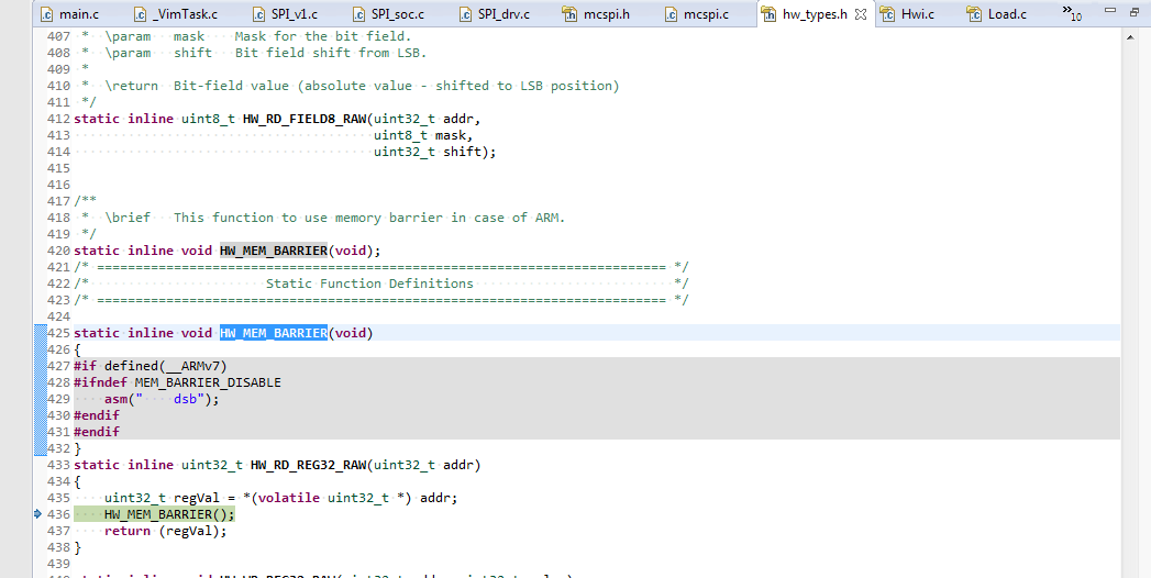
Since I know I'm not defining the symbol MEM_BARRIER_DISABLE, I have been happily assuming that this  asm("dsb");  was executing.  However, just while ago in stepping into this code, I saw this on my screen:

And suddenly realized that the symbol  __ARMv7  was not being defined, though I understand that the Cortex-A8 in the AM3358 is an ARMv7 processor.

4 questions:

Q1:  Given the above (MMU register memory ranges set for  bufferable == false  combined with the fact that that DSB instruction isn't being executed), what is ACTUALLY happening inside my processor and the L1 & L2 cache?

Q2:  Should I be defining the __ARMv7 symbol in my project?

Q3:  Is the data barrier instruction only needed when the MMU is set to cache register address ranges?

Q4:  Why in the hw_types.h code are there data barrier instructions on REGISTER READs?  I thought (possibly erroneously) that any type of external memory read would read straight through the L1/L2 cache (regardless of MMU settings) and thus the L1/L2 cache would be properly synchronized on ALL reads, and only at risk of being out of sync on CPU writes to external memory (thus the need for the data barrier instruction).  Am I missing some basic information about what the DSB instruction actually does and why it is needed?

Kind regards,
Vic

  • P.S. DMA is not in use (yet) since I just needed to prove the connection at this stage, so:

    MCSPI_CH0CONF.DMAR == 0, and
    MCSPI_CH0CONF.DMAW == 0
  • The RTOS team have been notified. They will respond here.
  • "cacheable"/"bufferable" is obsolete ARMv4/v5 terminology, replaced in ARMv6/v7 by:

    1. memory type: normal, device, or strongly-ordered;
    2. for normal type only, L1 and L2 cache policy: non-cacheable, write-through, or write-back;
    3. for write-back policy only, allocation hint: read-allocate or read/write-allocate;
    4. for normal and device type, shareability-flag. For device type it is inverted (default is shareable) and non-shared device is obsolete in v7. Note that the cortex-A8 does not support external coherence hence setting the shareable-flag on normal memory merely forces the cache policy to non-cacheable (for both cache levels).

    The backwards compatibility mapping is defined as:

    ARMv4/v5 | ARMv6/v7
    CB | typepolicyalloc
    0 0 | s-o n/a n/a
    0 1 | device n/a n/a
    1 0 | normal write-through read-allocate
    1 1 | normal write-back read-allocate

    You can find an example of how I personally do MMU setup on the AM335x here.

    A dsb instruction has no direct effects on caches. It does however force any previously executed writes or cache maintenance instructions in progress to complete. Note however that for write-back cacheable memory, a write completes when it hits the cache. Also, on the am335x, a non-strongly-ordered write to anything on the L3 interconnect (which is nearly everything) completes as soon as it's accepted by the async fifo from the cortex-A8 subsystem to the L3.

    For example if you'd write some code into memory then prior to executing it you would need to do:
    1. clean data cache to point of unification (required only if L1 write-back cacheable)
    2. dsb nshst (to commit previous writes or cache clean)
    3. invalidate instruction cache to point of unification
    (both cache ops can be by address range or entire L1 cache)

    It is worth mentioning that the cortex-A8 is the first ARMv7 processor and behaves far more conservatively than most later processors, which means you can get away with fewer memory barriers. In particular, all non-Neon memory instructions execute strictly in order (ignoring write buffering) and my impression is that every strongly-ordered access behaves as if there are memory barriers before and after it. This should not be relied on in code that should be upward-compatible with later processors.

    Putting a memory barrier, let alone a dsb, after a read is almost never useful. In general you normally don't need memory barriers when accessing device or strongly-ordered memory. When you do need one, the code you showed is unsafe: there are no constraints being imposed on the inline asm other than requiring it to be emitted, but gcc is allowed to move it across memory accesses occurring before or after it. The correct implementation of a full data sync barrier would be asm( "dsb" ::: "memory" );

  • Dear Matthijs,

    Wow, the above information appears to be EXACTLY what I needed.  I wish I could hire you to be in the same room as me for about 20 minutes so I can get all this cleared up.  Lacking that, I would like to ask you to point me in the direction of some good references for the AM335x (and later) silicon -- I see that I'm going to have to go ahead and bite the bullet and FULLY study and understand how the L1/L2 caching works on the ARMv7.  I have studied DISK CACHING and I find MOST of those concepts apply to L1/L2 but there is some additional vocabulary involved that I haven't yet found good definitions for yet.  Some terms I'm pretty sure I have an incomplete or incorrect definition for are "allocate" (as in write- and read-allocate) and "strongly ordered".  Would you be so kind as to advise me where I can get clear, complete definitions for these, and from there I think I will be able to look up data (hopefully) on the ARM website to better understand what's going on here.

    The code in  mmu.c   is outstanding:  clear, clean, well documented and understandable (save the gap in understanding about caching and MMU I need to fill in as described above).

    From what I can tell, I am guessing that you only use the APP.CFG MMU stuff to get you past any  "firstFxns"  that need to access peripherals (have one 1), and from there you re-set-up your own MMU scheme after entering the  main()  function?  Am I close?

    Looking forward to your reply,
    Vic

  • P.S. It's not just a BETTER understanding I need, but rather a COMPLETE understanding, because I'm writing firmware for the automotive industry (specifically racing) and due to the nature of reliability needs in this area, I cannot allow things I don't fully understand NOW to cause problems later. :-)
  • P.P.S. I've spent HOURS looking into Caching already trying to understand it and the MMU, and I'm close, but have a definite gap in understanding around those terms I mentioned above.
  • P.P.P.S. Re-studying the caching section of the ARMv7 Architecture Reference Manual....
  • The cache allocation hint refers to when an access that misses cache causes that line to be allocated in cache. If it isn't allocated then the access simply bypasses cache. There's a trade-off there since allocating a line in cache is relatively expensive and usually requires that another line is evicted to make space, but it makes future accesses much cheaper. Normally reads are always allocated in cache since otherwise there's not much point in marking the memory cacheable, but for writes it may be more favorable to choose not to allocate them. It depends on the application workload.

    Later arm cores also added the ability to specify no-allocate, i.e. just check if it's in cache but never allocate it there if it isn't.

    Strongly-ordered is basically just a restricted variant of device type. In fact in ARMv8 it has been renamed to Device-nGnRnE... not sure if I consider that an improvement. Device-type in general can be viewed as more or less the hardware equivalent of the "volatile" qualifier in C, meaning every access is performed as requested without any "optimizations" that would be valid for normal memory but might not be for memory-mapped I/O. Strongly-ordered however has stricter ordering requirements and (at least in the A8) waits synchronously for each access to complete. It keeps things basically as simple as on microcontrollers and such, but the performance penalty is high.

    For the full details the official reference is indeed the ARM Architecture Reference Manual v7-A/R, although it's not a particularly easy read and afaik it changed to give the CPU greater liberties at some point (which doesn't yet apply to the A8).

    And I don't actually use StarterWare at all, I have a custom C++ codebase for baremetal code. A small part of it can be found in the include dir of this funky little project which actually runs on linux but directly accesses PRCM, the control module, and GPIO, hence uses my baremetal headers for that.

  • Hi, Matthijs!

    Excellent explanation of cache-line allocation, and now that makes a lot more sense, given the time trade-offs involved.  Thank you for that.

    Your description of "strongly-ordered" helped me figure out what my mental block on this was:  I was trying to "think with" -- not a missing definition or partial definition, but -- an incorrect definition for "ordered", where I was trying to mentally apply "ordered" as something to do with numerical ordering (and the use of the <, ==, and > numerical comparisons), or storing/accessing adjacent memory locations in sequence as a requirement of the remote device or module, but in fact it is in reference to the load and store ACTION SEQUENCE as it relates to memory access results:  ensuring that the full effects of the prior memory access instruction have indeed taken place by the time the next instruction executes so that that next instruction can correctly assume that something has occurred (e.g. a primary- or side-effect of reading or writing to an address)!  Thus, the TOTAL reason why memory-mapped peripheral registers would HAVE TO BE accessed in a strongly-ordered way.  (The relief I feel is tremendous!)  I just spent the last several hours in the Architecture Reference Manual trying to sort that out (among other things).  I FINALLY found the term "ordering" (after clearing that up here) used in the description of the DMB (Data Memory Barrier) Hint instruction:  "... is a memory barrier that ensures the ordering of observations of memory accesses."   And even more pertinent:  section A3.5 "Memory types and attributes and the memory order model".

    Re the ARM Architecture Reference Manual -- long and detailed though it may be, I do find it refreshingly precise!

    Re the idea of not using StarterWare:  after closely examining and fixing bugs in a couple of StarterWare drivers recently (namely SPI and Touchscreen, bugs found and fixes posted in the StarterWare forum), I've realized that (taking SPI as an example) in any SINGLE driver, the author is going to have to make some assumptions about the application which aren't always going to be true, and that aren't always going to be the most efficient approach (given the myriad of possible application needs for an SPI interface).  And in realizing that, I realized that I am going to need to write some of my own drivers for my particular application so that I can take advantage of knowledge of the application needs in order to gain more efficiency.

    By the way, we have similar coding standards when it comes to CLARITY (readability and understandability of code).  I've trained a few programmers in my time and have found that there is SO much you can tell about how a person thinks by looking at his/her code....   :-)

    Thank you for the outstanding tips and definitions, and especially for your time!  You definitely got me unstuck!!

    Kind regards,
    Vic

  • P.S. It appears that ARM Architecture Reference Manual section A3.8.2 "Ordering requirements for memory accesses" is even MORE pertinent! :-)