This thread has been locked.

If you have a related question, please click the "Ask a related question" button in the top right corner. The newly created question will be automatically linked to this question.

AM5716: Cannot access DSP L2 SRAM from DSP core using global address

Part Number: AM5716

Hello,

I've run into some unexpected behavior. The DSP L2 SRAM appears twice in the DSP memory map. There is a "local" address range that is only accessible by the DSP (0x80 0000 through 0x84 7FFF) and there is a "global" address range that is accessible by other peripherals like the ARM (0x4080 0000 through 0x4084 7FFF). The problem I am experiencing is that the DSP cannot read the L2 SRAM contents using the global address -- only the local address is working. The behavior is summarized as follows. Note that I am using the Memory Browser in CCS7 to make these observations.

  • DSP attempts to read or write location 0x80 0000 -- SUCCESS
  • ARM attempts to read or write location 0x4080 0000 -- SUCCESS (this location is clearly mapped to DSP address 0x80 0000)
  • DSP attempts to read or write location 0x4080 0000 -- FAILURE (read always returns zero, write has no effect)

My question is whether this is the expected behavior? Is it invalid to read address range 0x4080 0000 - 0x4084 7FFF from within the DSP core?

Thanks as always for your help!

Best regards,
Dave

  • Hi,

    "DSP subsystem internal resources. DSP accesses in ranges [0x0080_0000 – 0x01D1_7FFF] and [0x0800_0000 – 0x0801_FFFF] are performed locally within the DSP subsystem."

    This is clearly stated in section 2.6 from the AM572x TRM Rev. H. See Note 1 below Table 2-10.
  • Biser, thank you, I am familiar with that footnote. It explains that DSP accesses in those ranges will be performed within the DSP subsystem, but it does not indicate that there is anything invalid about accessing the DSP L2 SRAM from the L3_MAIN memory space, which is shown in that table to be memory mapped to DSP addresses 0x1400 0000 - 0xFFFF FFFF. The "global" DSP L2 SRAM address range falls into this L3_MAIN memory space and is not covered by the footnote.
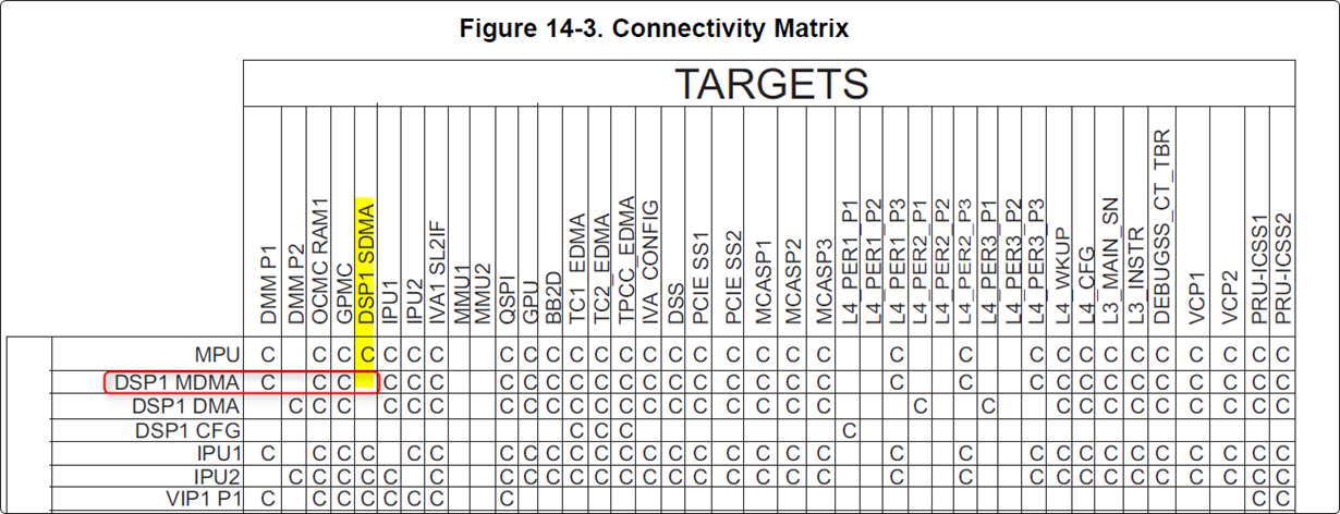
  • You cannot read from that address because there is no connection between the DSP's master port on the L3 (DSP MDMA) and the DSP's slave port on the L3 (DSP SDMA).  Here's the corresponding snippet from the interconnect chapter:

  • Brad, thank you for the clear explanation and reference. This is exactly what I was looking for!