This thread has been locked.

If you have a related question, please click the "Ask a related question" button in the top right corner. The newly created question will be automatically linked to this question.

RTOS/am5726: PCIe inbound write into external RAM fails

Part Number: AM5726

Tool/software: TI-RTOS

Hi,

  I'm  having DSP1 controlling the PCIe subsystem as 2xlan Gen2 RC. EP is a FPGA. RC Memory read requests are fine and also EP write requests work if the inbound memory target is DSPs local L2-RAM. But if I do the same with external DDR Memory, it fails.

The DSP is running on TI/RTOS with PDK 1.0.4 and sys/BIOS 6.46.0.23. It is booted via remoteproc from linux (processor-sdk-linux-rt-am57xx-evm-03.01.00.06) and has all necessary carveouts for the DDR memory region in its resource table. 

There are no errors regarding mmu fails (PCIe data path mmu is disabled), the request isn't rejected as unsupported - in fact everything seems to be quite nice, except the data never gets it into the memory.

Have I missed something? Do I have to give the PCIe subsystem any access rights for DDR? Since the L2 RAM address is a local one I have to convert it into global L3-Main address space. I don't need to do that for DDR-RAM addresses since it's already global - am I right?

Thanks in advance,

                                        Tim

  • The RTOS team have been notified. They will respond here.
  • Hi,

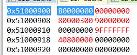
    One thing to check is the Linux also runs in DDR3, make sure the PCIE inbound doesn't conflict with Linux. Another is to check the PCIE inbound register setting: 0x51000900 to 0x0x51000920 via JTAG or devmem2, if this is PCIESS1.

    The typical one looks like attached picture, inbound direction, used the region 0. From 0x9000_0000 to 0x9000_0000, mapped to 0x4080_0000 (DSP local to global).

    In your case, the 0x5100_0918 would be something in DDR3. Does those registers look right?

    Regards, Eric

  • Eric,

      I think the ddr memory range in question doesn't conflict since there is already a carveout for the DSP in its resource table and it is excluded from linux memory map by stating following lines in the systems device tree config:

      reserved-memory {
        #address-cells = <2>;
        #size-cells = <2>;
        ranges;
    
        dsp1_cma_pool: dsp1_cma@99000000 {
          compatible = "shared-dma-pool";
          reg = <0x0 0x99000000 0x0 0x4000000>;
          reusable;
          status = "okay";
        };
    
      };


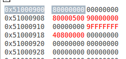
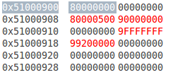
    The iATU registers seem ok to me:

    this is the set for DSP L2 RAM

    and this is the set for DDR RAM.

    The only difference to your settings is the 5 in the BAR_NUMBER field of  PCIECTRL_PL_IATU_REG_CTRL_2. But this shouldn't matter since MATCH_MODE is address, not BAR. 

    Hmm... out of luck still.

    Best,

      Tim

  • Tim,

    Yes, BAR number 3 or 5 doesn't matter. I tested two AM572X IDK EVM connected case with RTOS code. Then I edited one side 0x5100_0918 from 0x4080_0000 to 0x9920_0000, I was able to confirm that one side's 0x2100_0000 now mapped to 0x9920_0000 (instead of 0x0080_0000 previously) of the remote side, in DSP core's memory view window.

    So there is some setting in Linux preventing this... Let me check my Linux colleague.

    Regards, Eric
  • Tim,

    That carved out area can not be used by PCIe, but for IPC.

    Rex
  • Rex,

      as you may already have fiugred out, the address I point the pcie request to is not in the realm of IPC. The setup coming with the linux sdk has set the devmem section for IPC from 0x99000000 to 0x990FFFFF. I'm intentionally using a memory section 'behind' the one used by IPC, starting at 0x99100000 (buffer starts at 0x99200000).

    I already checked another setup with a carveout separated to the CMA-section defined in the linux device tree. the address was 0x90000000. I adapted the dsp resource table accordingly but to no avail.

    What makes you think that the OS running on the ARMs prevents the PCIe peripheral master port from writing to a memory location? What kind of a mechinsm is behind that?

    Best,

             Tim

  • Hi, Tim,

    Assuming the PCIe configuration in Linux is disabled, the possible causes which I can think of are either the data were written to different memory location or MMU didn't unblock it for DSP.

    For the first cause, you will need to be sure the inbound/outbound areas are aligned on both ends.

    In general, the resource table indicates which memory areas will be used by DSP. When the DSP image gets downloaded through remoteproc, remoteproc will get the info in the resource table and modify the MMU. This means 2 conditions, entry in resource table and downloading through remoteproc. From your post, it seems that you are using remoteproc to download, so that should have been taken care of.

    Rex
  • Hi Rex,

      sorry for the late response, I was AFK.

    Thanks for clarifying what could possibly go wrong from linux perspective.

    Unfortunately I'm still stuck:

    • The inbound/outbound areas are properly aligned:

    On FPGA side we work with 64bit PCIe address space so no outbound translation is necessary (and in the L2-RAM target case it's already working).

    On Sitara side the inbound translation maps from PCIe address 0x90000000 to DSP-L3-main address 0x90100000. in my understanding the alignment has to be on a 4kByte boundary which is hereby met.

    • The MMU doesn't block memory access.

    For example a local DMA transaction from PCIe address space into the questioned RAM area works fine and also CPU write accesses are working.

    I have tested once again with an address space completely separated from IPC devmem. Here is the list of carveouts/devmems of the resource table used for MMU programming by memproc:

    carveout: da:  40400000  pa:  00000000  len: 00100000
    carveout: da:  90000000  pa:  00000000  len: 00100000
    carveout: da:  90100000  pa:  00000000  len: 00d00000
    carveout: da:  90e00000  pa:  00000000  len: 00200000
    carveout: da:  9f000000  pa:  00000000  len: 00100000
    devmem:   da:  a0000000  pa:  99000000  len: 00100000
    devmem:   da:  80000000  pa:  ba300000  len: 05a00000
    devmem:   da:  60000000  pa:  a0000000  len: 0c000000
    devmem:   da:  70000000  pa:  70000000  len: 08000000
    devmem:   da:  78000000  pa:  78000000  len: 08000000
    devmem:   da:  02000000  pa:  02000000  len: 00100000
    devmem:   da:  20000000  pa:  20000000  len: 10000000
    devmem:   da:  51000000  pa:  51000000  len: 00800000
    devmem:   da:  4a000000  pa:  4a000000  len: 01000000
    devmem:   da:  48000000  pa:  48000000  len: 00200000
    devmem:   da:  48400000  pa:  48400000  len: 00400000
    devmem:   da:  48800000  pa:  48800000  len: 00800000
    devmem:   da:  54000000  pa:  54000000  len: 01000000
    devmem:   da:  4e000000  pa:  4e000000  len: 00100000

    The PCIe transfer target memory location in question is 0x90100000. The MMU maps it to the same address.

    If I fail to configure the resource table of the DSP firmware linux responds on illegal memory accesses with DSPs mmu0 dmesg error entries. This is not the case when the PCIe transfer fails.

    So, still out of luck. Any hints?

              Tim

    PS.: on linux side the whole PCIe bus is disabled. The DSP completely handles initialization and configuration of the PCIe subsystem. there is no pci entry anywhere below /sys filesystem.

  • Hi,

    I have a Linux with PCIE disabled on AM572x, can you send us the DSP firmware to be loaded by Linux (under /lib/firmware) for us to try. The DSP firmware need to configure PCIE PRCM and RC mode, also configure OB/IB translation and starts link training. We can setup another AM572x EVM as PCIE EP running standalone PCIE code to debug this (your firmware is expected to link up with our EP, then I can check translation to see why DDR can't be written on RC side).

    Regards, Eric
  • Good morning,

      I have a firmware ready. It configures itself as RC and tries to link 1 lane in gen2 mode. It doesn't configure any BARs and also no outbound translation on EP since that depends on EPs SW. If the EP writes to PCIe address 0x90000000 it should write to the local RCs address 0x90100000.

    Please let me know if anything else is needed.

    csxp.7z

  • Hi,

    I tried your DSP firmware. On the RC side, when the inbound mapped to OCMC (0x4080_0000) I can see the pattern written by EP using C66x. When the inbound mapped to DDR3 0x9010_0000, I can see the pattern from A15 (either using devmem2 or CCS memory view), but I can't see the pattern from DSP CCS CPU/Physical memory view. Is this your issue (do you use A15 or C66x to handle the received data from EP)?

    When you build the DSP firmware, there is a header file for resource table, can you share that file with us?

    Regards, Eric
  • Hi,

       thanks for testing - I had a look at the remoteproc driver code and had to learn that the implementation ignores the pa member of a carveout structure (I thought that's what the FW_RSC_ADDR_ANY macro is for). Luckily it's updated.

    I always thought of the resource table as a 'write only' structure and remoteproc has to try to follow the information it gets.

    I now successfully compute the base of the PCIe inbound address translation by reading the pa members of the carveouts.

    Now understanding the dynamic allocation of carveouts in Linux CMA space I wonder how I can allocate a carveout in eg OCMC space? How can I instruct remoteproc to use a certain CMA region for a certain carveout? My goal is to use a OCMC memory region for certain data to utilize several memory interfaces in parallel and have frequently needed data near to the DSP core. 

    Thanks again for your help,

                                   Tim

  • Tim,

    "I now successfully compute the base of the PCIe inbound address translation by reading the pa members of the carveouts."====> do you mean you have FPGA ----- PCIE ----- DSP writing into AM572x DDR working already?

    For the rest questions, we are working on it.

    Regards, Eric
  • Eric,

      yeah, it's working now! I thought I made remoteproc programming the DSP-mmu for a 1:1 address translation by stating a carveout in the resource table like this:

    struct fw_rsc_carveout {
        UInt32 type;
        UInt32 da;
        UInt32 pa;
        UInt32 len;
        UInt32 flags;
        UInt32 reserved;
        Char name[32];
    };
    
    struct fw_rsc_carveout ocmc2_caout =  {
              TYPE_CARVEOUT,
              OCMC2_RAM, 
              OCMC2_RAM,
              OCMC2_RAM_SIZE, 
              0, 
              0,
              "DSP_MEM_OCMC2",
          };

    I assumed with that carveout if I write eg to global address 0x40400000 the mmu would translate 1:1 to internal DSPs address 0x40400000. But I learned that the remoteproc driver places carveouts wherever linux finds a cma region, regardless of the 'pa'-member of struct fw_rsc_carveout. Note to myself: never assume anything. :)

    So in fact writing to the global DDR memory address via PCIe worked from the first minute, but from the DSP perspective I was always looking at the wrong address.

    Still eager to find out about intentionally using OCMC memory for a carveout... 

    And can you have a look at this thread again? The notification feature seems broken on this one, but I still have questions...

    Thanks a lot,

                    Tim

  • Still no answers?

    Please give a life sign to let me know there is something in process. we're running out of time and we don't want to temper with linux remoteproc code. Also see this thread I started in parallel because it seems to be a distinct question from the original intent of this thread.

  • Hi,

    Yesterday I tried to modify rsc_table.h to allocate code into OCMC and it worked (it runs previously in DDR), using M4. Not sure if the attached is helpful to you.rsc_table.h

    rsc_table.h.ori

    Regards, Eric

  • I don't understand. What have you changed in rsc_table.h to achieve that?!
    In my understanding the used physical memory is solely defined by the CMA from linux device tree where remoteproc is running on.
    Im working with processor sdk rt 3.1.0.6 don't know if remoteproc impelemtation has changed in a later release.
  • ah, ok now i understand that rsc_table.ori is the original one.
    So you say I have to define a devmem but give it the type carveout?!
    This seems odd to me but I will try.
  • Ok,

       I tried using a devmem entry with  type=carveout and basically the result looks the same as if I use a carveout entry with the same type.

    Here is the output of my application regarding the resources. Last Entry shows that the memory is mapped into the DDR-CMA:

    [ 0.0000] [0000_0022] Info: Resource Table:
    [ 0.0000] [0000_0091] Info: Carveout #0: DSP_MEM_TEXT 0x00100000 x 0x99100000 -> 0x90000000
    [ 0.0000] [0000_0207] Info: Carveout #1: DSP_MEM_DATA 0x00D00000 x 0x99200000 -> 0x90100000
    [ 0.0000] [0000_0323] Info: Carveout #2: DSP_MEM_HEAP 0x00200000 x 0x99F00000 -> 0x90E00000
    [ 0.0000] [0000_0438] Info: Carveout #3: DSP_MEM_IPC_DATA 0x00100000 x 0x9A100000 -> 0x9F000000
    [ 0.0000] [0000_0559] Info: Devmem #0: DSP_MEM_IPC_VRING 0x00100000 x 0x99000000 -> 0xA0000000
    [ 0.0000] [0000_0677] Info: Devmem #1: DSP_MEM_IOBUFS 0x05A00000 x 0xBA300000 -> 0x80000000
    [ 0.0000] [0000_0794] Info: Devmem #2: DSP_MEM_CMEM 0x0C000000 x 0xA0000000 -> 0x60000000
    [ 0.0000] [0000_0911] Info: Devmem #3: DSP_TILER_MODE_0_1 0x08000000 x 0x70000000 -> 0x70000000
    [ 0.0000] [0000_1032] Info: Devmem #4: DSP_TILER_MODE_2 0x08000000 x 0x78000000 -> 0x78000000
    [ 0.0000] [0000_1152] Info: Devmem #5: DSP_PCIE_MSI 0x00100000 x 0x02000000 -> 0x02000000
    [ 0.0000] [0000_1267] Info: Devmem #6: DSP_PCIE_SS1_MEM 0x10000000 x 0x20000000 -> 0x20000000
    [ 0.0000] [0000_1386] Info: Devmem #7: DSP_PCIE_SS1_CFG 0x00800000 x 0x51000000 -> 0x51000000
    [ 0.0000] [0000_1506] Info: Devmem #8: DSP_PERIPHERAL_L4CFG 0x01000000 x 0x4A000000 -> 0x4A000000
    [ 0.0000] [0000_1629] Info: Devmem #9: DSP_PERIPHERAL_L4PER1 0x00200000 x 0x48000000 -> 0x48000000
    [ 0.0000] [0000_1753] Info: Devmem #10: DSP_PERIPHERAL_L4PER2 0x00400000 x 0x48400000 -> 0x48400000
    [ 0.0000] [0000_1877] Info: Devmem #11: DSP_PERIPHERAL_L4PER3 0x00800000 x 0x48800000 -> 0x48800000
    [ 0.0000] [0000_2002] Info: Devmem #12: DSP_PERIPHERAL_L4EMU 0x01000000 x 0x54000000 -> 0x54000000
    [ 0.0000] [0000_2125] Info: Devmem #13: DSP_PERIPHERAL_DMM 0x00100000 x 0x4E000000 -> 0x4E000000
    [ 0.0000] [0000_2247] Info: Devmem #14: DSP_MEM_OCMC2 0x00100000 x 0x9A200000 -> 0x40400000

    Here is my Device tree (note that I improved the structure a bit so it comes in header and code file.

    #ifndef _CORE_RESOURCES_H_
    #define _CORE_RESOURCES_H_
    
    #include <ti/ipc/remoteproc/rsc_types.h>
    
    #define CORE_CARVEOUT_NUM 4
    #define CORE_DEVMEM_NUM   15
    
    #define CORE_RESOURCES_NUM (CORE_CARVEOUT_NUM + CORE_DEVMEM_NUM + 2)
    
    struct csxp_resource_table {
        struct resource_table    base;
    
        uint32_t offset[CORE_RESOURCES_NUM];  /* Should match 'num' in actual definition */
    
        /* rpmsg vdev entry */
        struct fw_rsc_vdev       rpmsg_vdev;
        struct fw_rsc_vdev_vring rpmsg_vring0;
        struct fw_rsc_vdev_vring rpmsg_vring1;
    
        /* carveout entries */
        struct fw_rsc_carveout   cout[CORE_CARVEOUT_NUM];
        /* trace entry */
        struct fw_rsc_trace      trace;
        /* devmem entries */
        struct fw_rsc_devmem     devmem[CORE_DEVMEM_NUM];
    };
    
    extern struct csxp_resource_table ti_ipc_remoteproc_ResourceTable;
    
    
    #ifdef __cplusplus
    extern "C" {
    #endif
    
    uint32_t core_loc2glob (uint32_t addr);
    void     core_print_mem_entries (void);
    
    #ifdef __cplusplus
    }
    #endif /* extern "C" */


    #endif /* _CORE_RESOURCES_H_ */
    

    #include <ti/csl/csl_chipAux.h>
    
    #include "util.h"
    #include "core_resources.h"
    #include "logging.h"
    
    
    /* DSP Memory Map */
    #define L4_DRA7XX_BASE          0x4A000000
    
    #define L4_PERIPHERAL_L4CFG     (L4_DRA7XX_BASE)
    #define DSP_PERIPHERAL_L4CFG    0x4A000000
    
    #define L4_PERIPHERAL_L4PER1    0x48000000
    #define DSP_PERIPHERAL_L4PER1   0x48000000
    
    #define L4_PERIPHERAL_L4PER2    0x48400000
    #define DSP_PERIPHERAL_L4PER2   0x48400000
    
    #define L4_PERIPHERAL_L4PER3    0x48800000
    #define DSP_PERIPHERAL_L4PER3   0x48800000
    
    #define L4_PERIPHERAL_L4EMU     0x54000000
    #define DSP_PERIPHERAL_L4EMU    0x54000000
    
    #define L3_PERIPHERAL_DMM       0x4E000000
    #define DSP_PERIPHERAL_DMM      0x4E000000
    
    #define L2_SRAM                 0x00800000
    #define L2_SRAM_SIZE            0x00048000
    
    #define OCMC2_RAM               0x40400000
    #define OCMC2_RAM_SIZE          0x00100000
    
    #define PCIE_MSI_MEMORY_BASE    0x02000000
    #define PCIE_MSI_MEMORY_SIZE    SZ_1M
    
    #define PCIE_SS1_MEMORY_BASE    0x20000000
    #define PCIE_SS1_MEMORY_SIZE    SZ_256M
    
    #define L3_PCIE_SS1_CFG_BASE    0x51000000
    #define DSP_PCIE_SS1_CFG_BASE   0x51000000
    
    #define L3_PERIPHERAL_ISS       0x52000000
    #define DSP_PERIPHERAL_ISS      0x52000000
    
    #define L3_TILER_MODE_1         0x70000000
    #define DSP_TILER_MODE_1        0x70000000
    
    #define L3_TILER_MODE_2         0x78000000
    #define DSP_TILER_MODE_2        0x78000000
    /* Co-locate alongside TILER region for easier flushing */
    #define DSP_MEM_IOBUFS          0x80000000
    
    #define DSP_MEM_TEXT            0x90000000
    #define DSP_MEM_DATA            0x90100000
    #define DSP_MEM_HEAP            0x90E00000
    #define DSP_MEM_CMEM            0x60000000
    
    //0x85900000
    #define DSP_SR0_VIRT            0xBFD00000
    #define DSP_SR0                 0xBFD00000
    
    #define DSP_MEM_IPC_DATA        0x9F000000
    #define DSP_MEM_IPC_VRING       0xA0000000
    #define DSP_MEM_RPMSG_VRING0    0xA0000000
    #define DSP_MEM_RPMSG_VRING1    0xA0004000
    #define DSP_MEM_VRING_BUFS0     0xA0040000
    #define DSP_MEM_VRING_BUFS1     0xA0080000
    
    #define DSP_MEM_IPC_VRING_SIZE  SZ_1M
    #define DSP_MEM_IPC_DATA_SIZE   SZ_1M
    
    #define DSP_MEM_IOBUFS_SIZE     (SZ_1M * 90)
    
    #define DSP_MEM_TEXT_SIZE       (SZ_1M *   1)
    #define DSP_MEM_DATA_SIZE       (SZ_1M *  13)
    #define DSP_MEM_HEAP_SIZE       (SZ_1M *   2)
    #define DSP_MEM_CMEM_SIZE       (SZ_1M * 192)
    
    /*
     * Assign fixed RAM addresses to facilitate a fixed MMU table.
     */
    /* This address is derived from current IPU & ION carveouts */
    #define PHYS_MEM_IPC_VRING      0x99000000
    
    /* Need to be identical to that of IPU */
    #define PHYS_MEM_IOBUFS         0xBA300000
    #define PHYS_MEM_CMEM           0xA0000000
    
    /*
     * Sizes of the virtqueues (expressed in number of buffers supported,
     * and must be power of 2)
     */
    #define DSP_RPMSG_VQ0_SIZE      256
    #define DSP_RPMSG_VQ1_SIZE      256
    
    /* flip up bits whose indices represent features we support */
    #define RPMSG_DSP_C0_FEATURES         1
    
    
    extern char ti_trace_SysMin_Module_State_0_outbuf__A;
    #define TRACEBUFADDR (UInt32)&ti_trace_SysMin_Module_State_0_outbuf__A
    
    #pragma DATA_SECTION(ti_ipc_remoteproc_ResourceTable, ".resource_table")
    #pragma DATA_ALIGN(ti_ipc_remoteproc_ResourceTable, 4096)
    
    struct csxp_resource_table ti_ipc_remoteproc_ResourceTable = {
        1,                      /* we're the first version that implements this */
        CORE_RESOURCES_NUM,     /* number of entries in the table */
        0, 0,                   /* reserved, must be zero */
        /* offsets to entries */
        {
            offsetof(struct csxp_resource_table, rpmsg_vdev),
            offsetof(struct csxp_resource_table, cout[0]),
            offsetof(struct csxp_resource_table, cout[1]),
            offsetof(struct csxp_resource_table, cout[2]),
            offsetof(struct csxp_resource_table, cout[3]),
            offsetof(struct csxp_resource_table, trace),
            offsetof(struct csxp_resource_table, devmem[0]),
            offsetof(struct csxp_resource_table, devmem[1]),
            offsetof(struct csxp_resource_table, devmem[2]),
            offsetof(struct csxp_resource_table, devmem[3]),
            offsetof(struct csxp_resource_table, devmem[4]),
            offsetof(struct csxp_resource_table, devmem[5]),
            offsetof(struct csxp_resource_table, devmem[6]),
            offsetof(struct csxp_resource_table, devmem[7]),
            offsetof(struct csxp_resource_table, devmem[8]),
            offsetof(struct csxp_resource_table, devmem[9]),
            offsetof(struct csxp_resource_table, devmem[10]),
            offsetof(struct csxp_resource_table, devmem[11]),
            offsetof(struct csxp_resource_table, devmem[12]),
    offsetof(struct csxp_resource_table, devmem[13]), offsetof(struct csxp_resource_table, devmem[14]) }, /* rpmsg vdev entry */ { TYPE_VDEV, VIRTIO_ID_RPMSG, 0, RPMSG_DSP_C0_FEATURES, 0, 0, 0, 2, { 0, 0 }, /* no config data */ }, /* the two vrings */ { DSP_MEM_RPMSG_VRING0, 4096, DSP_RPMSG_VQ0_SIZE, 1, 0 }, { DSP_MEM_RPMSG_VRING1, 4096, DSP_RPMSG_VQ1_SIZE, 2, 0 }, { { TYPE_CARVEOUT, DSP_MEM_TEXT, 0, DSP_MEM_TEXT_SIZE, 0, 0, "DSP_MEM_TEXT", }, { TYPE_CARVEOUT, DSP_MEM_DATA, DSP_MEM_DATA, DSP_MEM_DATA_SIZE, 0, 0, "DSP_MEM_DATA", }, { TYPE_CARVEOUT, DSP_MEM_HEAP, 0, DSP_MEM_HEAP_SIZE, 0, 0, "DSP_MEM_HEAP", }, { TYPE_CARVEOUT, DSP_MEM_IPC_DATA, 0, DSP_MEM_IPC_DATA_SIZE, 0, 0, "DSP_MEM_IPC_DATA", } }, { TYPE_TRACE, TRACEBUFADDR, 0x8000, 0, "trace:dsp", }, { { TYPE_DEVMEM, DSP_MEM_IPC_VRING, PHYS_MEM_IPC_VRING, DSP_MEM_IPC_VRING_SIZE, 0, 0, "DSP_MEM_IPC_VRING", }, { TYPE_DEVMEM, DSP_MEM_IOBUFS, PHYS_MEM_IOBUFS, DSP_MEM_IOBUFS_SIZE, 0, 0, "DSP_MEM_IOBUFS", }, { TYPE_DEVMEM, DSP_MEM_CMEM, PHYS_MEM_CMEM, DSP_MEM_CMEM_SIZE, 0, 0, "DSP_MEM_CMEM", }, { TYPE_DEVMEM, DSP_TILER_MODE_1, L3_TILER_MODE_1, SZ_128M, 0, 0, "DSP_TILER_MODE_0_1", }, { TYPE_DEVMEM, DSP_TILER_MODE_2, L3_TILER_MODE_2, SZ_128M, 0, 0, "DSP_TILER_MODE_2", }, { TYPE_DEVMEM, PCIE_MSI_MEMORY_BASE, PCIE_MSI_MEMORY_BASE, PCIE_MSI_MEMORY_SIZE, 0, 0, "DSP_PCIE_MSI", }, { TYPE_DEVMEM, PCIE_SS1_MEMORY_BASE, PCIE_SS1_MEMORY_BASE, PCIE_SS1_MEMORY_SIZE, 0, 0, "DSP_PCIE_SS1_MEM", }, { TYPE_DEVMEM, L3_PCIE_SS1_CFG_BASE, DSP_PCIE_SS1_CFG_BASE, SZ_8M, 0, 0, "DSP_PCIE_SS1_CFG", }, { TYPE_DEVMEM, DSP_PERIPHERAL_L4CFG, L4_PERIPHERAL_L4CFG, SZ_16M, 0, 0, "DSP_PERIPHERAL_L4CFG", }, { TYPE_DEVMEM, DSP_PERIPHERAL_L4PER1, L4_PERIPHERAL_L4PER1, SZ_2M, 0, 0, "DSP_PERIPHERAL_L4PER1", }, { TYPE_DEVMEM, DSP_PERIPHERAL_L4PER2, L4_PERIPHERAL_L4PER2, SZ_4M, 0, 0, "DSP_PERIPHERAL_L4PER2", }, { TYPE_DEVMEM, DSP_PERIPHERAL_L4PER3, L4_PERIPHERAL_L4PER3, SZ_8M, 0, 0, "DSP_PERIPHERAL_L4PER3", }, { TYPE_DEVMEM, DSP_PERIPHERAL_L4EMU, L4_PERIPHERAL_L4EMU, SZ_16M, 0, 0, "DSP_PERIPHERAL_L4EMU", }, { TYPE_DEVMEM, DSP_PERIPHERAL_DMM, L3_PERIPHERAL_DMM, SZ_1M, 0, 0, "DSP_PERIPHERAL_DMM", }, { TYPE_CARVEOUT, OCMC2_RAM, OCMC2_RAM, OCMC2_RAM_SIZE, 0, 0, "DSP_MEM_OCMC2", }, } }; uint32_t core_loc2glob (uint32_t addr) { int i; if (addr < 0x20000000) /* GPMC space - core specific local address */ return (1UL << 30) | (CSL_chipReadReg(CSL_CHIP_DNUM) << 24) | (addr & 0x00FFFFFFUL); for (i = 0; i < ARRLEN(ti_ipc_remoteproc_ResourceTable.cout); i++) { if (addr - ti_ipc_remoteproc_ResourceTable.cout[i].da < ti_ipc_remoteproc_ResourceTable.cout[i].len) return addr - ti_ipc_remoteproc_ResourceTable.cout[i].da + ti_ipc_remoteproc_ResourceTable.cout[i].pa; } for (i = 0; i < ARRLEN(ti_ipc_remoteproc_ResourceTable.devmem); i++) { if (addr - ti_ipc_remoteproc_ResourceTable.devmem[i].da < ti_ipc_remoteproc_ResourceTable.devmem[i].len) return addr - ti_ipc_remoteproc_ResourceTable.devmem[i].da + ti_ipc_remoteproc_ResourceTable.devmem[i].pa; } return addr; } void core_print_mem_entries () { int i; struct fw_rsc_carveout * cout; struct fw_rsc_devmem * dmem; LogMsgPush(LM_CSXP, LL_Info, "Resource Table:\n"); for (i = 0, cout = &ti_ipc_remoteproc_ResourceTable.cout[0]; i < ARRLEN(ti_ipc_remoteproc_ResourceTable.cout); i++, cout++) LogMsgPush(LM_CSXP, LL_Info, "\tCarveout #%d: %s 0x%08X x 0x%08X -> 0x%08X\n", i, cout->name, cout->len, cout->pa, cout->da); for (i = 0, dmem = &ti_ipc_remoteproc_ResourceTable.devmem[0]; i < ARRLEN(ti_ipc_remoteproc_ResourceTable.devmem); i++, dmem++) LogMsgPush(LM_CSXP, LL_Info, "\tDevmem #%d: %s 0x%08X x 0x%08X -> 0x%08X\n", i, dmem->name, dmem->len, dmem->pa, dmem->da); }

  • Hi,

       I'm a bit confused by the silence here. Is there any activity on your side regarding my questions? It would be great to have a clue if it's worth to wait for a response...

    Best,

            Tim

  • Tim,

    Sorry I didn't understand this well. Your goal is to add an entry to allocate some memory buffer from OCMC instead of DDR. Then you added a devmem entry and type is carveout, then it worked already. Isn't it? And you said: [ 0.0000] [0000_2247] Info: Devmem #14: DSP_MEM_OCMC2 0x00100000 x 0x9A200000 -> 0x40400000 this is still from DDR?

    Regards, Eric
  • Eric,

      'Your goal is to add an entry to allocate some memory buffer from OCMC instead of DDR. '

    this is correct.

      'Then you added a devmem entry and type is carveout, then it worked already. '

    Unfortunately this is not correct. When I try to map the OCMC as DEVMEM of type DEVMEM and place a data section in it remoteproc fails to load the program segments:

    [   74.268170] omap-rproc 40800000.dsp: assigned reserved memory node dsp1_cma@99000000
    [   74.280798]  remoteproc2: 40800000.dsp is available
    [   74.287296]  remoteproc2: Note: remoteproc is still under development and considered experimental.
    [   74.296986]  remoteproc2: THE BINARY FORMAT IS NOT YET FINALIZED, and backward compatibility isn't yet guaranteed.
    [   74.535471]  remoteproc2: powering up 40800000.dsp
    [   74.540320]  remoteproc2: Booting fw image dra7-dsp1-fw.xe66, size 6289932
    [   74.563617] omap_hwmod: mmu0_dsp1: _wait_target_disable failed
    [   74.569519] omap-iommu 40d01000.mmu: 40d01000.mmu: version 3.0
    [   74.577414] omap-iommu 40d02000.mmu: 40d02000.mmu: version 3.0
    [   74.611649]  remoteproc2: bad phdr da 0x92000000 mem 0xb8180
    [   74.617341]  remoteproc2: Failed to load program segments: -22
    [   74.641688] omap_hwmod: mmu1_dsp1: _wait_target_disable failed
    [   74.655405] omap_hwmod: mmu0_dsp1: _wait_target_disable failed
    [   74.661302]  remoteproc2: rproc_boot() failed -22
    [   74.667540] virtio_rpmsg_bus: probe of virtio0 failed with error -22
    [   74.674639]  remoteproc2: registered virtio0 (type 7)
    

    When I try to map the OCMC as DEVMEM of type CARVEOUT and place a data section in it remoteproc loads the program but places the carveout into CMA area, means the physical address member of the devmem structure is ignored and remoteproc uses the DDR RAM again.

    [     0.0000] [0000_0018] Debug: Resource Table:
    [     0.0000] [0000_0131] Debug:        Carveout #00: 0x00100000 x 0x99100000 -> 0x90000000 DSP_MEM_TEXT
    [     0.0000] [0000_0358] Debug:        Carveout #01: 0x00D00000 x 0x99200000 -> 0x90100000 DSP_MEM_DATA
    [     0.0000] [0000_0582] Debug:        Carveout #02: 0x00200000 x 0x99F00000 -> 0x90E00000 DSP_MEM_HEAP
    [     0.0000] [0000_0809] Debug:        Carveout #03: 0x00100000 x 0x9A100000 -> 0x9F000000 DSP_MEM_IPC_DATA
    [     0.0000] [0000_1043] Debug:        Devmem #00: 0x00100000 x 0x99000000 -> 0xA0000000 DSP_MEM_IPC_VRING
    [     0.0000] [0000_1272] Debug:        Devmem #01: 0x05A00000 x 0xBA300000 -> 0x80000000 DSP_MEM_IOBUFS
    [     0.0000] [0000_1495] Debug:        Devmem #02: 0x0C000000 x 0xA0000000 -> 0x60000000 DSP_MEM_CMEM
    [     0.0000] [0000_1712] Debug:        Devmem #03: 0x08000000 x 0x70000000 -> 0x70000000 DSP_TILER_MODE_0_1
    [     0.0000] [0000_1944] Debug:        Devmem #04: 0x08000000 x 0x78000000 -> 0x78000000 DSP_TILER_MODE_2
    [     0.0000] [0000_2171] Debug:        Devmem #05: 0x00100000 x 0x02000000 -> 0x02000000 DSP_PCIE_MSI
    [     0.0000] [0000_2389] Debug:        Devmem #06: 0x10000000 x 0x20000000 -> 0x20000000 DSP_PCIE_SS1_MEM
    [     0.0000] [0000_2617] Debug:        Devmem #07: 0x00800000 x 0x51000000 -> 0x51000000 DSP_PCIE_SS1_CFG
    [     0.0000] [0000_2844] Debug:        Devmem #08: 0x01000000 x 0x4A000000 -> 0x4A000000 DSP_PERIPHERAL_L4CFG
    [     0.0000] [0000_3080] Debug:        Devmem #09: 0x00200000 x 0x48000000 -> 0x48000000 DSP_PERIPHERAL_L4PER1
    [     0.0000] [0000_3317] Debug:        Devmem #10: 0x00400000 x 0x48400000 -> 0x48400000 DSP_PERIPHERAL_L4PER2
    [     0.0000] [0000_3556] Debug:        Devmem #11: 0x00800000 x 0x48800000 -> 0x48800000 DSP_PERIPHERAL_L4PER3
    [     0.0000] [0000_3796] Debug:        Devmem #12: 0x01000000 x 0x54000000 -> 0x54000000 DSP_PERIPHERAL_L4EMU
    [     0.0000] [0000_4039] Debug:        Devmem #13: 0x00100000 x 0x4E000000 -> 0x4E000000 DSP_PERIPHERAL_DMM
    [     0.0000] [0000_4275] Debug:        Devmem #14: 0x00100000 x 0x9A200000 -> 0x40400000 DSP_MEM_OCMC2
    

      'And you said: [ 0.0000] [0000_2247] Info: Devmem #14: DSP_MEM_OCMC2 0x00100000 x 0x9A200000 -> 0x40400000 this is still from DDR?'

    yep, the debug output format is size x physical address -> device address (mmu-mapped). Even when using a devmem entry in the resource table: if I set its type to CARVEOUT remoteproc uses the same mechanism for memory allocation as if I use a carveout entry with same type. Means: it uses CMA region in DDR Memory for allocation and ignores the physical address member of the resource entry.

    But my recent tests raise a fundamental question: is it even worth to use OCMC? I did some memory tests and see the same bandwidth for DMAs on DDR and OCMC. Only on random access I see a slightly better performance using OCMC. I searcht for it but to avail: Is there some benchmark data available regarding memory Bandwidth for DSPs L1, L2, OCMC and DDR3 for the am572X?

    Best,

                  Tim


  • I might be too late to this thread and I am not sure I completely understand what has been done/tried, but I can share my experience with an almost identical setup. I also have the DSP core using PCIe directly as the RC talking to an FPGA as the EP. The FPGA has an internal DMA capability, so when the FPGA has data ready for the DSP it sends the data via PCIe and the DSP gets an MSI interrupt. My original plan was to send the data to the OCMC RAM, but it appeared that that RAM was cached. So after every transfer I would have to have done a cache invalidate to get the DSP to be able to see the data the FPGA put into the OCMC RAM. The reason I wanted to used the OCMC RAM was because the L2SRAM was not large enough to hold my destination buffer. (We collect a bunch of FPGA Packets then process them later.) The cache invalidate seemed to really slow things down, so my current working solution was to create a small buffer in the L2SRAM (the non-cached area) just big enough for one packet from the FPGA, then upon the MSI interrupt copy from L2SRAM buffer to DDR3 buffer. This seems to be working just fine with no manual cache operations. Also, there is no Linux interaction needed and nothing special in the resource table.
  • Also, about the Failed to load program segments: -22 error. I think this happens when you define an area in the DSP memory that is outside the normal program/data area of your DSP. Remote proc tries to initialize the area like it would any DSP memory, but I'm not sure things are really all setup yet and it fails. My solution to that is to not declare the buffer in the DSP at all. Rather, declare a pointer to the memory area you want use. This way the DSP image does not actually contain any sections at that memory and remote proc won't attempt to initialize it. I think you can use the L2SRAM though as the MMU is not required to access that from the DSP.
  • Hi Christopher,

      thanks for sharing!

    We are about to decide if we do the transactions the way you do - with FPGA as requester and MSI as complete signal. However, we would target DDR RAM since our overall payload is around 4MBytes.

    I switched off cache for the regions I use for prefetching: L2-RAM and OCMC. In light of the problems getting memproc to allocate carveouts from certain memory regions I already go with pointers to OCMC combined with a OCMC DEVMEM entry in the resource table. That works well but one has to do the memory allocation management at runtime. It would be more safe to let the compiler do what it's meant to do.

    I'm am surprised that I can access OCMC by pointer even without a resource table entry. I've been under the impression that there always has to be an address translation to take place, otherwise an address translation fault would occur. Quite a bit shady what remoteproc does with the dsp mmu. I'll have a look at it at runtime, maybe there is a bypass region defined I don't know of.

    But that aside, what are the achieved bandwidths on your side, Chistopher?

    And I'm still interested in memory benchmarks regarding OCMC and DDR on am572x though... :)

    Best,

                Tim

  • Sorry Tim we have not done any max bandwidth testing.  The system performs well enough as is to meet our timeline, data transfer wise at least, so we just have not studied the actual PCIe transfer rate.