This thread has been locked.

If you have a related question, please click the "Ask a related question" button in the top right corner. The newly created question will be automatically linked to this question.

BEAGLEBN: PRU EGPIO timing

Part Number: BEAGLEBN

Hi,

I use the PRUs in a BeagleBone. PRU software is written in clpru 2.2.1.

I can not reach the timing goals for my project.

Debugging leads to the result that a simple write-read-back on the GPIOS need 40ns to complete, not 10ns as expected.

Test setup: I toggle an R30 output pin and wait until the voltage level re-appears on R31.

Code:

while (1) {
__R30 |= (1 << 12); // set PRU1.12
while (!(__R31 & 0x80)) ; // wait until readback on DATAIN7
__R30 &= ~(1 << 12); // clear PRU1.12
while (__R31 & 0x80); // wait until readback on DATAIN7
}

The logic analyzer shows that a single

__R30 |= (1 << 12); // set PRU1.12
while (!(__R31 & 0x80)) ; // wait

needs 40 nano seconds.


I  can generate a good square wave at 66MHz with

while(1) {
__R30 |= (1 << 12); // 5ns
__R30 &= ~(1 << 12); // 5ns
}

so the "while (!(__R31 & 0x80)) ;" part needs 35ns.

http://processors.wiki.ti.com/index.php/AM335x_PRU_Read_Latencies says: EGPIO read is 1 cycle = 5ns.

The BeagleBone itself apparently does not contain an low passes.

What could causes a delay of 7 cycles on EGPIO R31 read?

thanks for caring,
Joerg Hoppe,  PEAK System Technik GmbH

  • Hi,

    Apparently it's the "while" loop that's taking the extra cycles. You should check the assembly code generated by the compiler.
  • Biser,

    thanks for answering so fast.

    I verified the ASM code again. Thanks to clpru -O3 optimization, the while loop is just a one-line (line # 166), overhead 5ns.

    See extract from the listing:

         145;----------------------------------------------------------------------
         146; 162 | __R30 |= (1 << 12); // set PRU1.12                                     
         147;----------------------------------------------------------------------
         148 00000004 0000001F0CFEFE          SET       r30, r30, 0x0000000c  ; [ALU_PRU] |162|
         149;* --------------------------------------------------------------------------*
         150;*   BEGIN LOOP ||$C$L2||
         151;*
         152;*   Loop source line                : 163
         153;*   Loop closing brace source line  : 164
         154;*   Known Minimum Trip Count        : 1
         155;*   Known Maximum Trip Count        : 4294967295
         156;*   Known Max Trip Count Factor     : 1
         157;* --------------------------------------------------------------------------*
         158 00000008                 ||$C$L2||:    
         159;***    -----------------------g3:
         160;*** 163        -----------------------    if ( !(__R31&0x80u) ) goto g3;
         161        .dwpsn  file "pru1_buslatches.c",line 163,column 10,is_stmt,isa 0
         162;----------------------------------------------------------------------
         163; 163 | while (!(__R31 & 0x80))                                                
         164; 164 |         ; // wait until readback on DATAIN7                            
         165;----------------------------------------------------------------------
         166 00000008 000000C907FF00          QBBC      ||$C$L2||, r31, 0x07  ; [ALU_PRU] |163|


    Meanwhile I tried to calculate the frequency response of the PRU direct inputs.
    According to datasheet
               sprs717j.pdf, Chapter 7.14.1.1,
    the GPIO-Inputs are loaded with 30pF max internally.
    The outputs can drive 6mA at 3.3V, so assume they have 500 ohm (static DC)
    with f = 1 / (2 * pi * R *C) I calculate a low pass frequency of
    1 / (6.3 * 500 * 30E-12) = 10MHz, resulting in period of 100ns
    As I measured 40ns for a single Low/High level to be read back, this is about the same dimension.
         
    If the intern lowpass is the explanation for my delay, then you'd need to drive the PRU direct inputs with
    a impedance of about 50 Ohm to reach 100MHz. Would you agree?

    However, this was just a test setup. My real circuitry drives the PRU inputs with 74LVT541 bus drivers, which can drive 50mA (instead of 6mA in the test). This would result in R=66 ohm and in a cut off frequency of 80MHz, but I have the same 40ns response time there.

    thanks again,

    Joerg Hoppe, PEAK System technik GmbH


  • Hello Joerg,

    Are you using the default Direct input mode for the GPIs, or a different mode?

    Regards,
    Nick
  • Nick,

    I'm not sure what you mean with "mode".. perhaps here is something to learn?

    My software uses simple parallel input/ouptut :  no local PRU multiplexing, no shift register.

    In fact I did not set any PRU config registers, beside the initalization in clpru'ss ""_c_int00_noinit_noargs" startup" routine.

    The value for the pad config (pin multiplexing) register is 0x2e:

    SLEWCTRL 0x40 =0 : fast

    RXACTIVE  0x20 = 1: input receiver active

    PULLUDEN 0x8 = 1: pullups/pulldown disabled

    thanks for answering,

    Joerg

  • Hello Joerg,

    1) To make sure you are in Direct Input mode:
    Check out AM335x TRM section "PRU Module Interface to PRU I/Os and INTC", especially subsection "General-Purpose Inputs (R31): Enhanced PRU GP Module". General-purpose input mode Direct Input will be faster than input mode 16-Bit Parallel Capture.

    I would not expect it to take 8 clocks for loopback to occur with Direct Input mode. I am digging more into the hardware to get a better idea of what should be expected.

    2) I'm trying to get a better idea of loading: on the beaglebone, you are connecting a wire from pin PR1_PRU1_PRU_R30_12 to pin PR1_PRU1_PRU_R31_7, and making no other changes? On your board, what is the loopback setup you are using with the 74LVT541 bus drivers?

    FYI, your 66MHz example makes sense:
    while(1) {
    __R30 |= (1 << 12); // 5ns
    __R30 &= ~(1 << 12); // 5ns
    } // branch takes 5ns

    Regards,
    Nick
  • I am also a bit unclear on your application. Are you doing a PRU_GPO to PRU_GPI loopback, or something else? What does it look like?

    I would be curious to see your measured waveform. Without looking at the assembly, I would expect the logical low part of your waveform to be an extra clock cycle more than the logical high due to the branch/jump instruction at the bottom of the while loop.

    Regards,
    Nick
  • Nick,

    Thanks for your input.

    > 1) Assert Direct Input Mode.

    A input mode of "16-bit parallel capture" would explain a longer input read time. But I don't think this is the problem.

    - As I read spruh73n, chapter 4.4.1.2.3.2, I'd need a clock signal at GPI16 PRU1_16 to see any input in "parallel cpature" mode.
    - I understand that GPCFG1<1:0> = PRU1_GPI_MODE must be 0 for direct input mode.
    Via "pru_cfg.h" this is done by a "CT_CFG.GPCFG1_bit.PRU1_GPI_MODE = 0" now.
    Behaviour did not change.

    > 2) I'm trying to get a better idea of loading: on the beaglebone, you are connecting a wire from pin PR1_PRU1_PRU_R30_12 to pin PR1_PRU1_PRU_R31_7, and making no other changes?
    > On your board, what is the loopback setup you are using with the 74LVT541 bus drivers?

    For the tests, I cut off R31.7 and connect it directly to R30.12, which is a otherwise unconnected testpoint just for debugging. So in fact its just a R30.12 - R31.7 wire, without influence by my circuits. On the BBB however R31.7 is P8.40 and this is connected to some more components.
    I ordered another BBB and a prototype cape and will setup the "readback loop" as separate project.

    3) The 66MHz wave generated by 

    while(1) {
    __R30 |= (1 << 12); // 5ns
    __R30 &= ~(1 << 12); // 5ns
    } // branch takes 5ns

    is one cycle H and two cycles L, as expected:

    > 4) I am also a bit unclear on your application.
    > Are you doing a PRU_GPO to PRU_GPI loopback, or something else? What does it look like?

    Its gonna be a device emulator for vintage parallel computer bus (DEC PDP-11 UNIBUS).

    My circuit contains an 64-to-8 input multiplexer. 64 inputs go to eight 74lvth541 input latches. Output of all latches is connected to an internal 8 bit bus,
    read by PRU1_GPI<0:7>. To read a single latch, PRU1.GPO<8:10> outputs the address (0..7) to a "3-to-8" decoder 74AC138 which enables the selected latch
    to drive PRU1_GPI<0:7>.

    I noticed that the cycle from "address output" to "latch input read" takes considerably more time than calculated from the latencies of 74ac138 and 74lvth541.

    I debugged that down to the fact that reading an PRU1 input is slower than expected, this is demonstrated by the "write-readback"  test described here.

    The wave form of the loopback test

    while (1) {
    __R30 |= (1 << 12); // set PRU1.12
    while (!(__R31 & 0x80)) ; // wait until readback on DATAIN7
    __R30 &= ~(1 << 12); // clear PRU1.12
    while (__R31 & 0x80); // wait until readback on DATAIN7
    }

    is:

    best regards,

    Joerg

  • Nick,

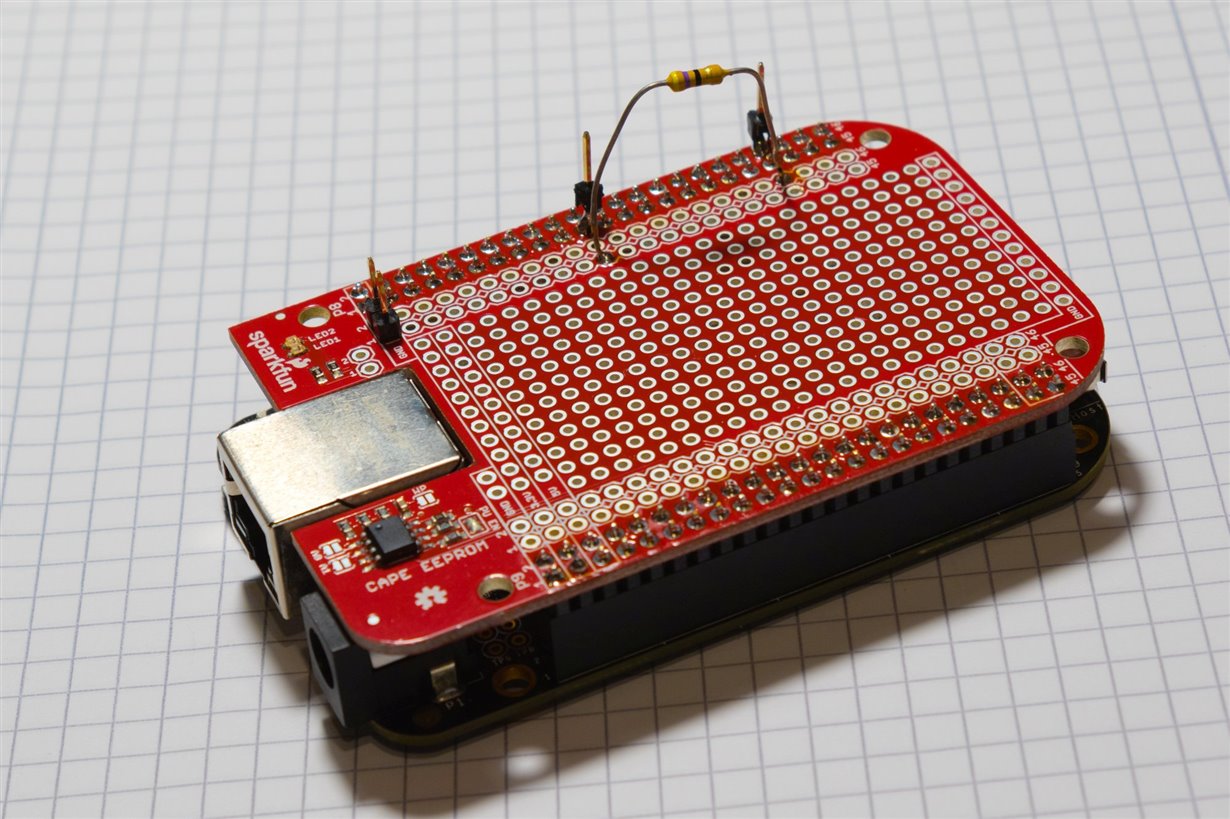
    I repeated the "loopback" test with a new BBB and this prototype cape:

    https://www.sparkfun.com/products/12774


    Output P8.21 = PRU1.GPO12 was connectect on shortest way to input P8.40 = PRU1.GPI7
    Results:
    - connection with a plain wire: 35ns delay
    - connection with an optimized resistor of 33 ohm: 30ns

    The single inline resistor serves as terminator, damping over/undershoots. See Graham&Johnson's "High Speed Digital Design: A Handbook of Black Magic".

    As I measured 40ns delay on my primary circuit, we can attribute a delay of at least 10ns  to trace routing and signal shape.

    I couldn't get the delay lower than 30ns = 6 cycles with this setup.

    At least this made clear again: the PRUs are so fast, we have to take high-frequency signal behaviour into account.

    Maybe we start a competition:

    ***   Who can get the "loopback" delay faster than 30ns?  ***

    thanks for reading this,
    Joerg

  • Hello Joerg,

    Could you post photos of your three BeagleBone Black setups that resulted in the three different latencies? I've started a discussion with our hardware engineers, but they are having trouble visualizing the differences between setups.

    I'll do a test on this end to see if I can replicate your results.

    Regards,
    Nick
  • Hi Nick,

    here are two pictures.

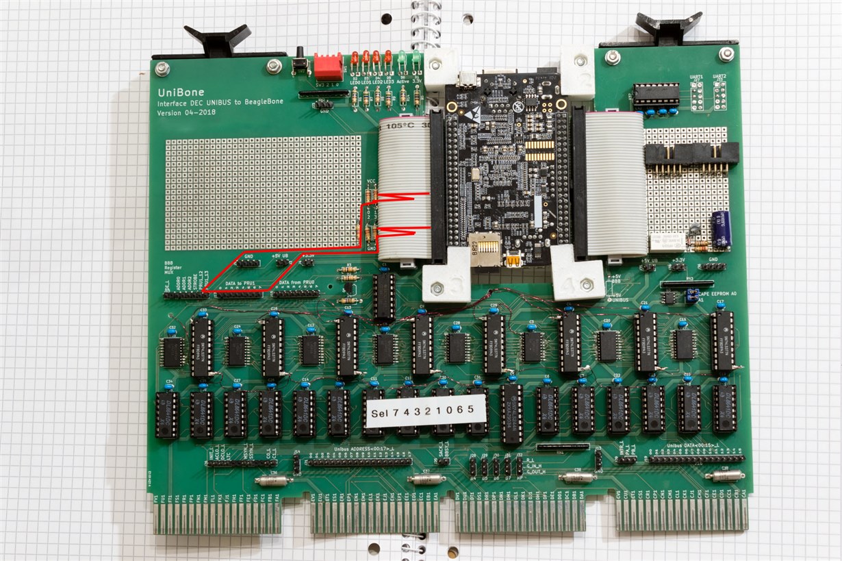
    1.) The "green" board is the project I'm working on ("UniBone"). I marked the trace routing of the loopback in RED.

    Loopback is PRU1.GPO[12] (BBB header P8.21) to PRU1.GPI[7] (BBB header P8.40) .

    The signal travels some distance on the board and runs through about 2 inches of folded flat cable without any thermination.

    A delay of 40 nano seconds is measured.

    2) The same loopback is made on the red prototype cape. Loopback is here realized with a short 47 ohm resistor. resulting in approx 30ns delay.

    3) Replacing the 47 ohm with a "zero-ohm" wire results in 35ns delay. I did not add a picture of this again ... would look not really different.

    Joerg

  • Hello Joerg,

    I am sorry for the delayed response. From the hardware team:

    Capacitive load will slow the transition. So the scope probe capacitance could add delay.

    It is not possible to tell if the entire signal path on the board shown in the first photo is routed as a impedance controlled transmission line. However, I suspect they have not maintained constant impedance going through the ribbon cable and ribbon cable connector. They definitely did not on the board shown in the second photo.

    The signal may have large over-shoots/under-shoots when it is not routed as a impedance controlled transmission line. If so, it may take a while for them to settle to a valid logic level. This could provide inconsistent results without delaying the input sample long enough for the signal to settle.

    I have not had time to run tests on my side yet. Let me know if you want more support on this.

    Regards,
    Nick
  • Hello Nick, and all,

    Nick Saulnier said:
    From the hardware team:

    Capacitive load will slow the transition. So the scope probe capacitance could add delay.

    It is not possible to tell if the entire signal path on the board shown in the first photo is routed as a impedance controlled transmission line. However, I suspect they have not maintained constant impedance going through the ribbon cable and ribbon cable connector. They definitely did not on the board shown in the second photo.

    The signal may have large over-shoots/under-shoots when it is not routed as a impedance controlled transmission line. If so, it may take a while for them to settle to a valid logic level. This could provide inconsistent results without delaying the input sample long enough for the signal to settle.

    I know the first prototype on the 1st picture is a mess, regarding signal quality.
    So lets work only on the reduced "loop-back" setup on the 2nd picture.

    I understand your hardware team is suspecting bad impedance match between PRU outputs, PRU inputs, and perhaps the logic analyzer probe.
    I agree, signal quality must be corrected first.

    From my measurements I found the 47 Ohm terminator on the 2nd picture (direct PRU input-output loop back) reduces overshoots/undershoots enough.
    I may be wrong and will concentrate on wave forms again (may take some time).

    Can your hardware team give a link on "How to build a impedance controlled transmission line suitable for the BeagleBone PRU inputs"?
    Or draw a sketch of recommended circuitry for the 2nd board setup?

    The BBB designers known more about their board, perhaps they already made a  "PRU loop-back" test and have a solution. Can you build up a contact?

    This information would be of interest to anybody working with the PRUs in highspeed applications.

    thanks again for all your effort,
    Joerg


  • Hello Joerg,

    I think impedance control would be more an issue of messy signal transitions rather than contributing to the overall latency how long it takes for the signal to travel. That could involve design choices like interspersing signal wires with ground wires in the ribbon cable.

    In terms of the loopback test, using a short u shaped wire resulted in 30 ns on this side (when observing with a scope). That could be increased to 35 ns or 40 ns by using a wire that was several inches longer.

    Regards,
    Nick

    EDIT 8/15/2018: test code was

  • Hi Nick,

    I understand right: you reproduced the 30ns (=6 cycle) delay in a BeagleBone PRU EGPIO loopback ?

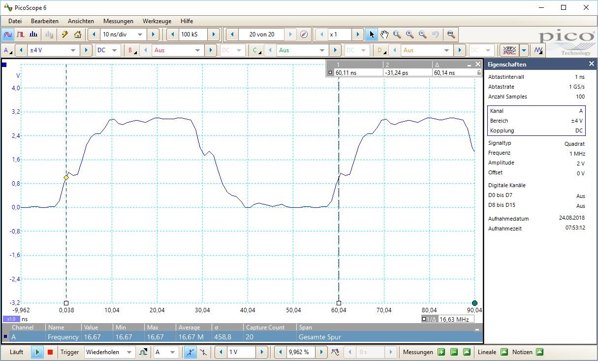
    I finally did some measurement, with a 47 ohm loop back resistor and a zero ohm loobback.  The scope is rated only 200MHz, but comparing both signals indicate overshoot/undershoot is not the problem, at least not with 47 ohm.

    Do you have any ideas how to proceed? Or is the BBB just "working as designed"?

    best regards,

    Joerg

    Attachment: waveforms.

    a) with a 47Ohm loopback (as on the pictures before)

    b) with a zero ohm wire:

  • Hello Joerg,

    Yes, it looks like this is the expected delay. Here is an estimate of about what the silicon designer would expect the timing to look like:

    end of R30 write (at 0 ns) -> IO delay (3ns) -> PCB delay (1ns) -> IO delay (2ns) -> synchronization flop (5ns) -> R31 read (5 ns) -> R30 write to toggle (5ns)

    Based on his input, I would be surprised to see a loopback result of less than 25ns for your test. 30 ns sounds reasonable.

    It sounds like the best way to reduce the loopback delay would be to reduce the trace length.

    If you need to reduce the time even more (and have the time to sink into it), there may be software elements of your design which can be sped up. For example, if the ARM requests the PRU to change the latches, you may be able to speed up that communication protocol.

    Regards,
    Nick
  • Nick,

    thanks to you and your collegues for that thoroughly research.

    Maybe I optimize the software to use the EGPIOs in an overlapping manner. I can first send new signals on R31, then read back previous ones over R30.

    I think we can close this issue.

    best regards,

    Joerg