Hi Team,
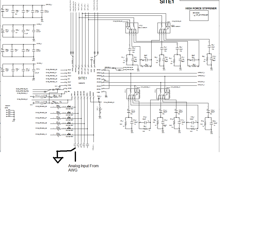
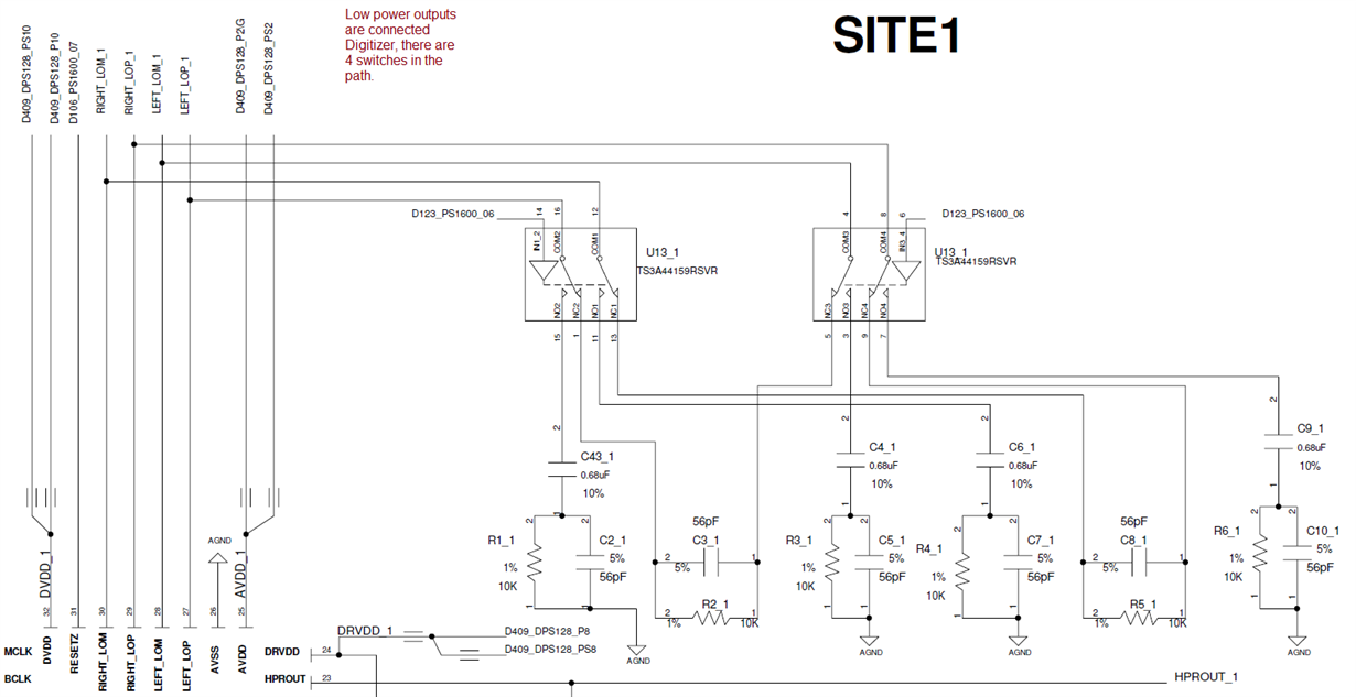
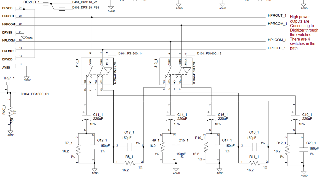
I am using the above part to check the Leakage current for the power supply pins (DRVDD, AVDD, IOVDD and DVDD), for AVDD pin reading higher current than expected for other pins currents are in the limits.
Below procedure fallowed to check the leakage current.
1. Power on the device (AVDD = DRVDD = IOVDD = 3.3V & DVDD = 1.8V).
2. Run "Reset pattern" ( Pattern includes setting the Reset pins "Low" for 650ns and setting Reset pin "High" for 650ns. and measure the current across the power supply pins.
3. After reset we could see measured current are within the limits.
4. Run "Power patten" , In Power pattern setting the below registers.
| REGISTER ADDRESS | DATA | |
| 0000 0111(07) | 0010 1010(2A) | 1.fS(ref) = 48 kHz 2.ADC dual-rate mode is disabled 3.DAC dual-rate mode is enabled 4.Left-DAC data path plays left-channel input data 5.Right-DAC data path plays right-channel input data |
| 0010 0101(37) | 1100 0000(C0) | 1.Left and right DAC is powered up 2.HPLCOM configured as differential of HPLOUT |
| 0010 1001(41) | 0101 0000(50) | 1.Left-DAC output selects DAC_L3 path to left line output driver 2.Right-DAC output selects DAC_R3 path to right line output driver 3.Left- and right-DAC channels have independent volume controls |
| 0010 1011(43) | 0000 0000(00) | 1.The left-DAC channel is not muted 2.Left-DAC Digital Volume Control Setting is set to 0dB |
| 0010 1100(42) | 0000 0000 (00) | 1.Output Driver Power-On Delay Control- Driver power-on time = 0 μs 2.Driver Ramp-Up Step Timing Control-Driver ramp-up step time = 0 ms |
| 0101 0110(86) | 0000 1001(09) | 1.LEFT_LOP/M Output Level Control is set to 0dB 2.LEFT_LOP/M is not muted 3.All programmed gains to LEFT_LOP/M have been applied 4.LEFT_LOP/M is fully powered up |
| 0101 1101(93) | 0000 1001(09) | 1.RIGHT_LOP/M Output Level Control is set to 0dB 2.RIGHT_LOP/M is not muted 3.All programmed gains to RIGHT_LOP/M have been applied 4.RIGHT_LOP/M is fully powered up |
5. On writing the register 86 and 93 causing the high current drawn at "AVDD" pins, below attached PPT
6. Especially on writing bit 0 that is power on both Right and Left Lop causing the high current.
Let me know on your suggestions.
Thanks & Regards,
Sunil BK


