This thread has been locked.

If you have a related question, please click the "Ask a related question" button in the top right corner. The newly created question will be automatically linked to this question.

LM5141-Q1 IC is too hot

Other Parts Discussed in Thread: LM5141

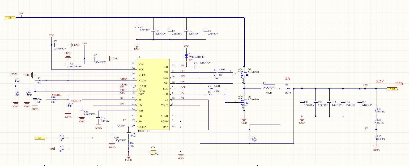
This is my second design LM5141,40V-5.2V DC-DC

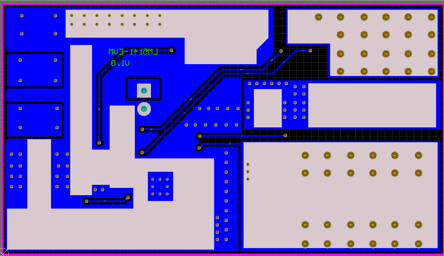
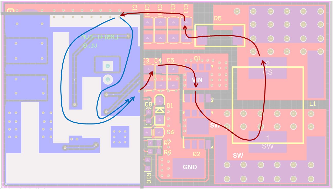
I design the EVM refer  to the WENBENCH tool schematic

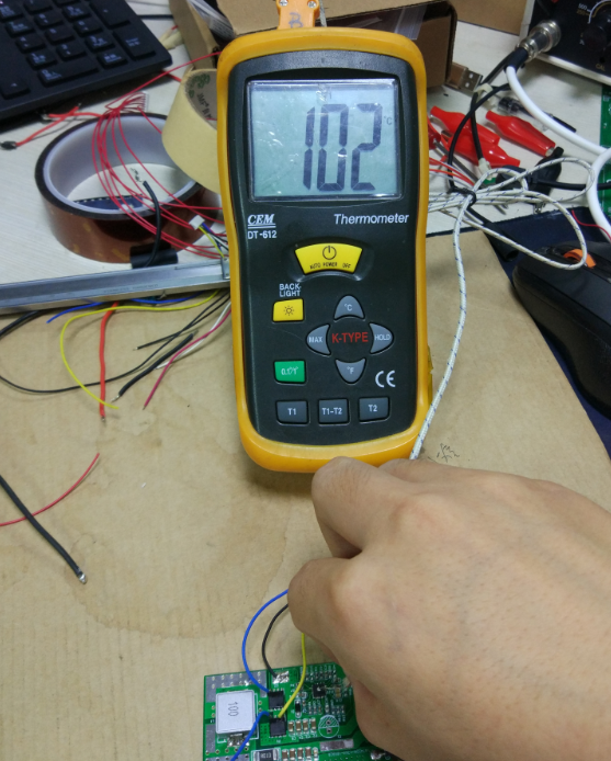
When input is 40V,output is 5.V 3A,IC and MOS are very hot,about 100℃,

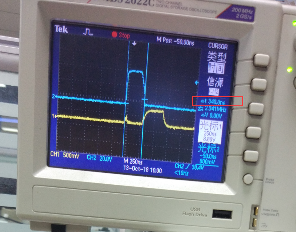
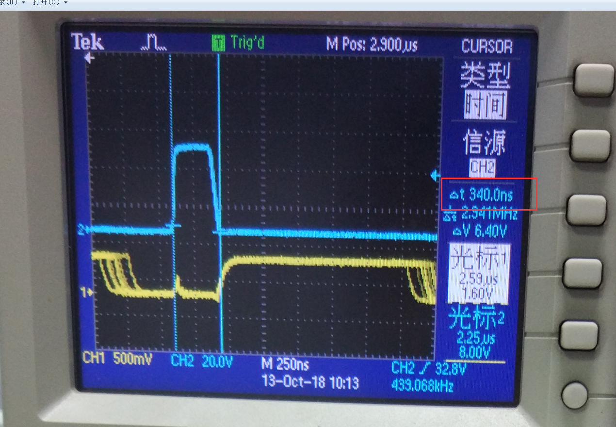
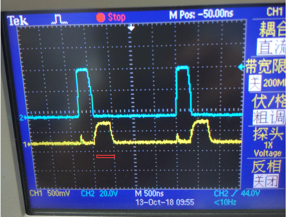
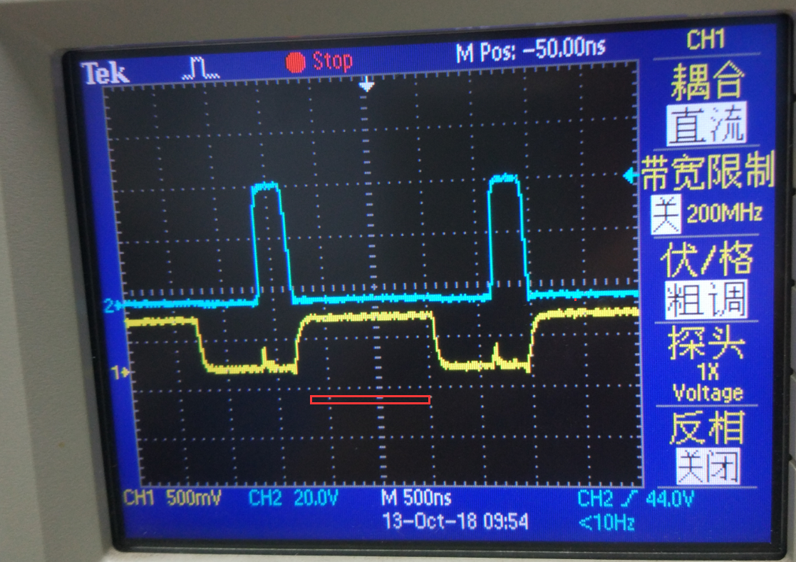
Here are there picture about the high and low MOS driver waves,in different output current。

Blue diagram is high MOS driver

Yellow diagram iS low MOS driver

output is1A

output is 2A

output is3A

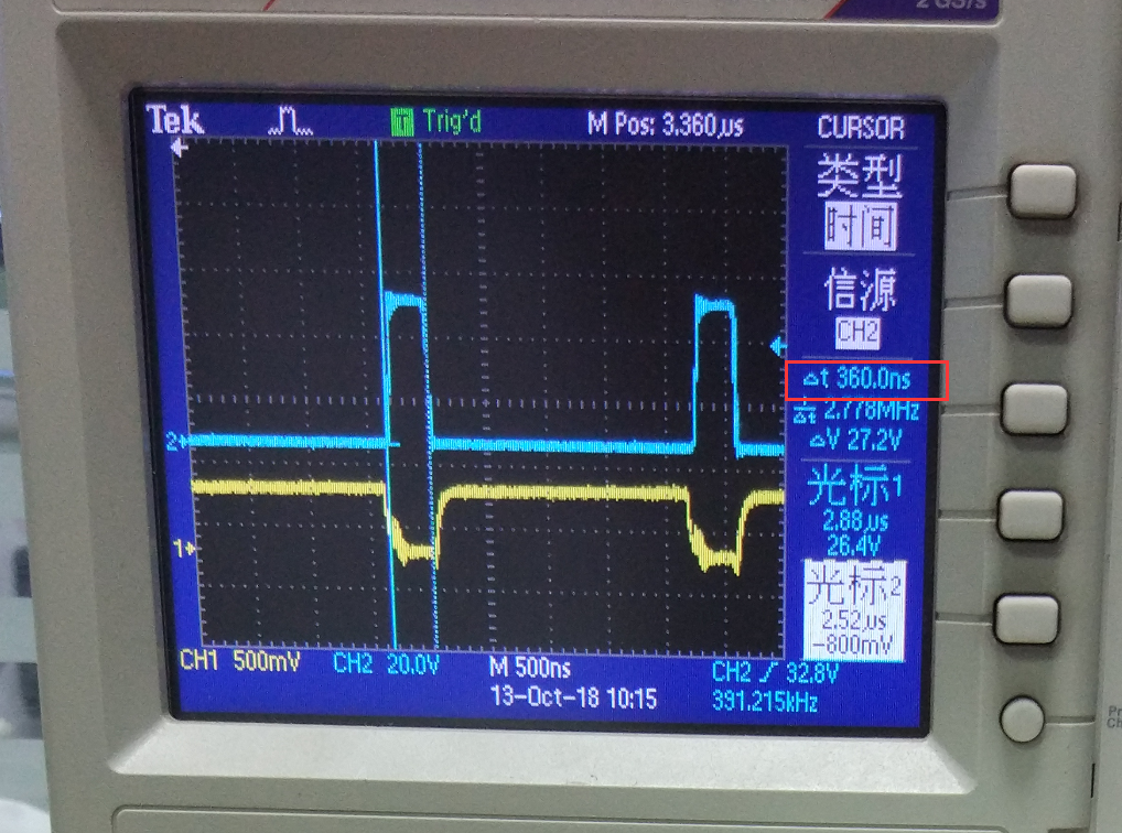
See the above there picture,when operate the different output current ,the high MOSFET driver open time almost keep unchanged

Let us see the low MOS diver wave changes in different output current

1A

2A

3A

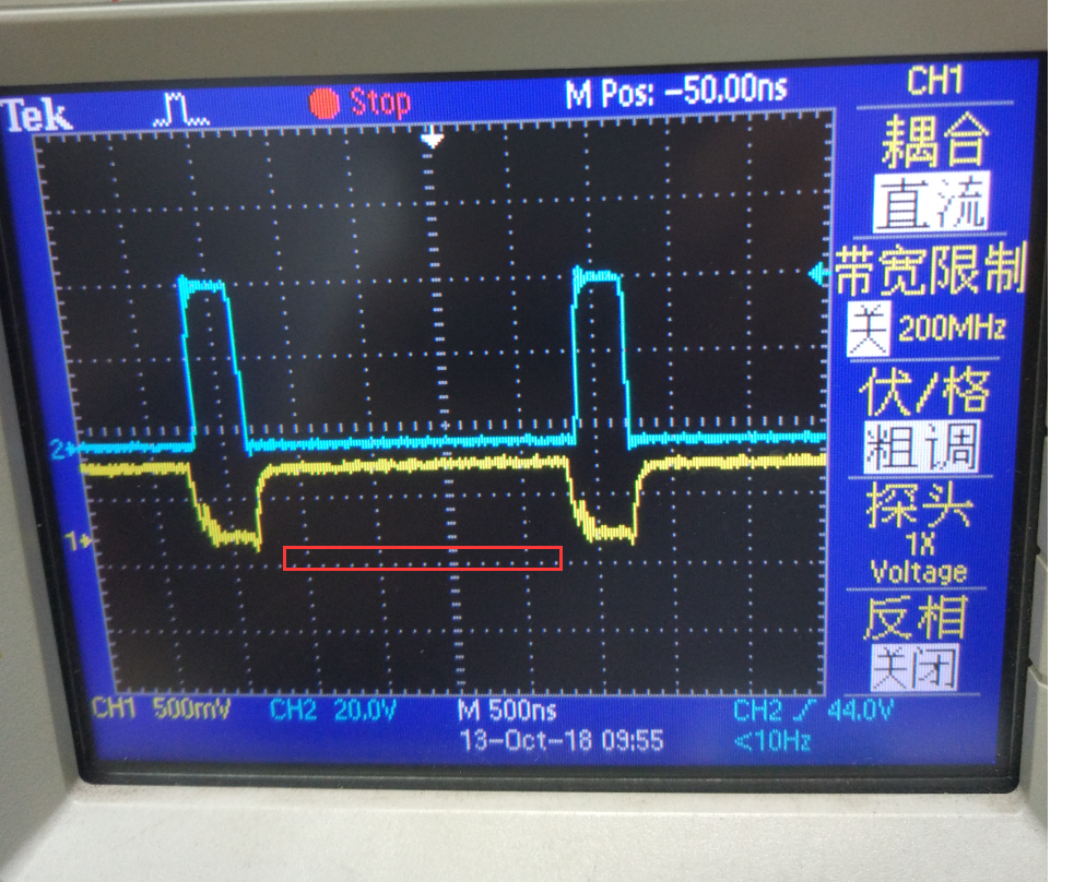
I am in interrogative ,as usual,when the loading is added,the high driver should gain the duty cycle in the buck circuit,Otherwise  this state  is not my hope, and  why only  the low driver duty cycle was added when the output current  was added 1A  to 3A? 

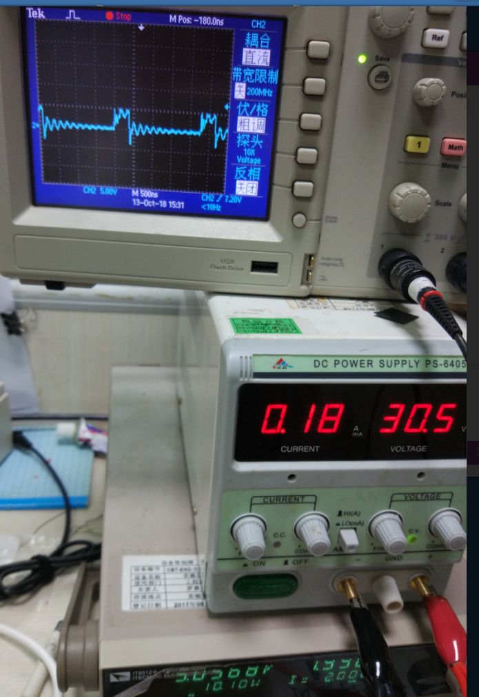
I have  test  the high MOS Vgs,the wave was very strange

It was seen like not as full work,I gusset if it is the reason why MOSFET was very hot,even the output is only 1A

So my main question is something case the IC and  MOSFET hot,I hope someone can help me to solve this problem

  • Hello,

    Thank you for sharing the detailed information about your design.

    The ground connection to the bottom of the board is very critical for heat dissipation.  I would recommend increasing the ground plane on the bottom of the board, similar to the EVM:

    I will also share your description with the product expert for any additional recommendations.

    Best Regards,

    Katelyn Wiggenhorn

  • thanks,I am sure that  IC GND is enough,because the IC is not  pover  device

    I found main reason was that high MOS driver is very weak when  the input over 20V 

    like this pictures:

    input is 12V,higt MOS Vgs is normal ,IC and MOS can't be hot

    input is 30V,higt MOS Vgs wave is Disorderly,IC and MOS are hot

    input is 40V,higt MOS Vgs wave is more in trouble

    the driver is very weak,so the MOS be  hot when load ,this state  I understand

    But  the IC be hot when input is higt voltage,and the driver wave can't serve MOS switch fully,

    So what case the IC can't work in high input voltage?

  • User,

    Thank you for all the detail. Here are my thoughts.

    1. The on-time should not change by much with increasing load. The duty cycle (ideally) is constant with a constant VIN and VOUT. Ton should only increase slightly due to power loss in the buck circuitry. The reason the Toff increases is because the low-side FET is only on while there is current in the inductor. Lighter load means IL reaches zero amps and the low-side FET turns off (diode emulation, DEMB pin connected to GND). Heavy load means IL doesn't reach zero amps so the low-side FET turns off when the high-side FET turns on (in your 3A waveform). So this is normal.

    2. It is very important that you use the tip-and-barrel method to take these measurements.

    3. I believe the thermal layout on the IC is good if the gray part is solid copper. It looks like it is. If not, extend the GND plane connected to the IC's thermal vias on the bottom-layer.

    4. Schematic looks good. Stable. Confirmed on WEBENCH.

    5. The layout looks okay at first look but one big thing that stood out to me was the placement of the output capacitors. The current has a long way to travel when going from COUT (GND pad) to CIN (GND pad). This may be causing issues. See picture (red arrows are top layer, blue are bottom layer). See the datasheet for more layout guidelines.

    6. It looks like the low-side is starting to turn on when the high-side turns on but it goes back to GND. That looks abnormal and may be due to the measuring technique but we should find out why it's there.

    7. Please also measure low-side gate like you measured high-side gate. Use a differential probe if you can. If not, use 2 channels (CH1 on gate, CH2 on source) and subtract gate from source.

    -Sam

  • Deer Sam:

      thank for  help  me analyse my circuit ,now I understand the how the low-side MOS ON-time changed when it be in Diffrent  current load!

    Point 5:I don't think the current path is too long

    Point 6: you said right ,low-side MOS be on a few time,when high-side MOS begin on,But I don't know how to test

  • User,

    Were you able to take/retake the data I suggested using the tip-and-barrel method?

    -Sam
  • Sam:

      I understand what you said,but which point shall I test? 

  • User,

    My thought was to retake the data you already took using the tip and barrel method. And also take the data I suggest above in part 7. But I just noticed something else.

    The VIN capacitor near the IC (C7) has a long path from VIN to the cap to GND of the IC. This loop should be very small. The large loop in the current layout would explain the bad gate drive waveform. Try removing C7, then place it on top of the IC and solder wires directly from the VIN pin to the cap and from the cap directly to the PGND pin just to test if this is the issue.

    You may also try increasing C7 from 0.47uF to 2.2uF or 4.7uF.

    -Sam

  • Hello,

    Due to inactivity, I am going to close this thread. If you have any additional questions, please open a new thread.

    Best Regards,
    Katelyn