This thread has been locked.

If you have a related question, please click the "Ask a related question" button in the top right corner. The newly created question will be automatically linked to this question.

TPA3118D2: TPA3118D2

Part Number: TPA3118D2

Hi,

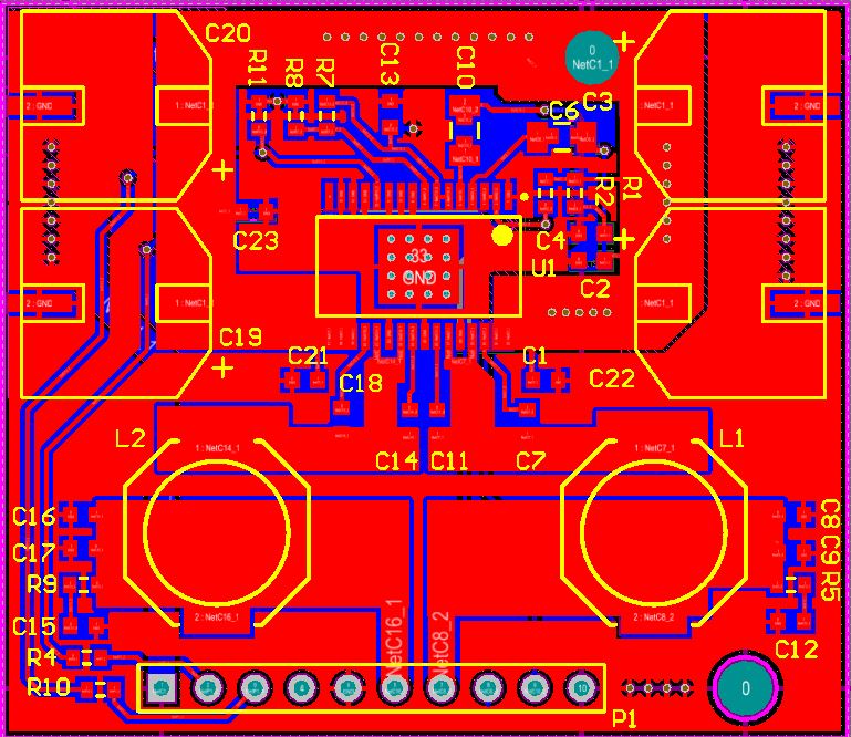
I am using TPA3118D2 in a PBTL (mono mode) as per datasheet page 26, figure 37 (bottom part only). I will try to attach the PCB layout as further information if this editor lets me.

My problem is it is generating too much EMI/ radiated noise ground of the PCB seems to be the worse case, PVCC seems to be ok but ground has a lot of noise on it which is causing EMC problems. looking at the ground noise with a spectrum analyser, I can see anything between 15-20dBuv noise at 150MHz. This noise is all over the PCB and causing problems. I dont mind so much the noise level, its the location of noise on the frequency band (150MHz), if it had the same noise level at higher or lower frequency I wouldnt mind but just cant have it where it is currently.

Noise existing on ground makes it difficult to make notch filters or traps. The PCB is my first prototype and I realise the output out of the chip and its output out of the inductor have a largish copper area, I will make these smaller on the next iteration - any tips on the layout would be great - on my list is lots of stitching to reduce impedance. I am also looking at TI's evaluation PCB to try to do a similar layout.

I am also trying to use ferrites to combat the radiation with their attenuation at around 150MHz, any other thing I should be looking at?

For now any help on reducing this ground noise and radiation would be great.

Thanks,

Sean

Below, current and new layouts.

  • Hi,

    I think the new PCB design is fine. The RE problem is related to current loop, the LC filter should be close to chip.

    You can also tune the caps C53 and C54 (page 26, figure 37 in datasheet). You can try to use 2.2nF caps for 150MHz spur. The 2 caps should be close to the connector.

    Hoping that can help you.

    Regards,

    Derek

  • Hi Derek,

    Thank you very much for your input.

    I will close up the distance between the inductors and output of chip to reduce the loop further.

    I will also have a go at tuning C53 & C54 as you suggest. How do you calculate the 2.2nF for 150MHz range?

    I have a pair of 330uF per PVCC  and another pair for AVCC as well as 100nF & 1nF in parallel. My input caps are 10uF.

    I find input lines like audio inputs and mute and shut down transfer a lot of EMI to the anything connected to these pins.

    I am also thinking of using these: The NFM21CC223R1H3D is a 2A/50VDC EMI Suppression Filter with 3-terminal capacitor which reduce residual inductance to an extremely low level making it excellent for noise suppression at high frequencies (Farnell: 1828797) on power line and speaker output lines. My maximum current is 1A.

    Would appreciate your thoughts.

    Regards,

    Sean

  • Hi Sean,

    I used the Murata Software tool "SimSurfing" to check the Impedance vs Frequency. I found the 2.2nF is fine for 150MHz spur.

    I think you can try to tune the caps value according to the test. From my experience, most customers can pass RE test by tuning the cas value.

    Regards,

    Derek

  • Hi Derek,

    Thanks very much again, will give it a try.

    My unit is going for marine environment so a lot more stringent at around 156-165MHz - limit line for the standard is 24dBuv!

    Regards,

    Sean