This thread has been locked.

If you have a related question, please click the "Ask a related question" button in the top right corner. The newly created question will be automatically linked to this question.

TLV320ADC3100: TLV320ADC3100

Part Number: TLV320ADC3100

Hi,

I am working on an audio project, I am using TLV320adc3100 for analog to digital conversion of the audio signal.

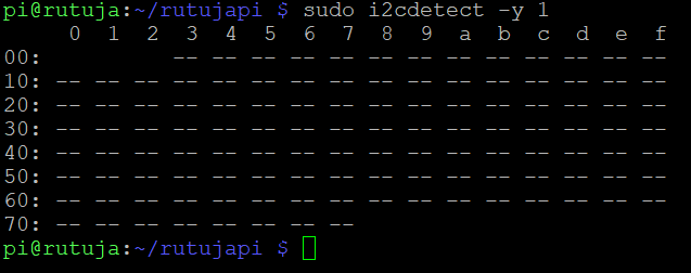
I am interfacing the adc with a raspberry pi (Host device) with i2c and configuring the registers as per my requirements in a python script using the read and write commands.

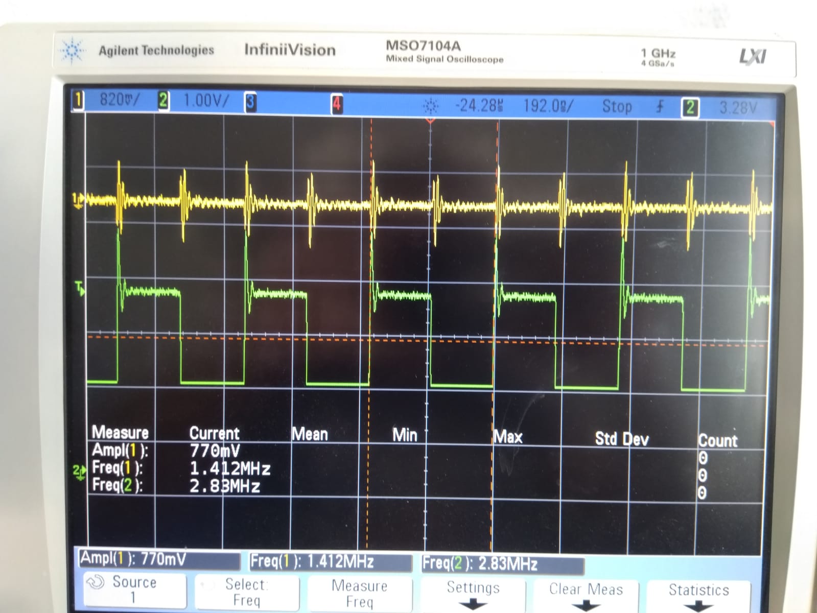
I want to use i2s format for serial communication.

Also, I am using the bclk(from i2s) as the pll clockin, and pll_clk as codec_clkin (configured via register 4). 

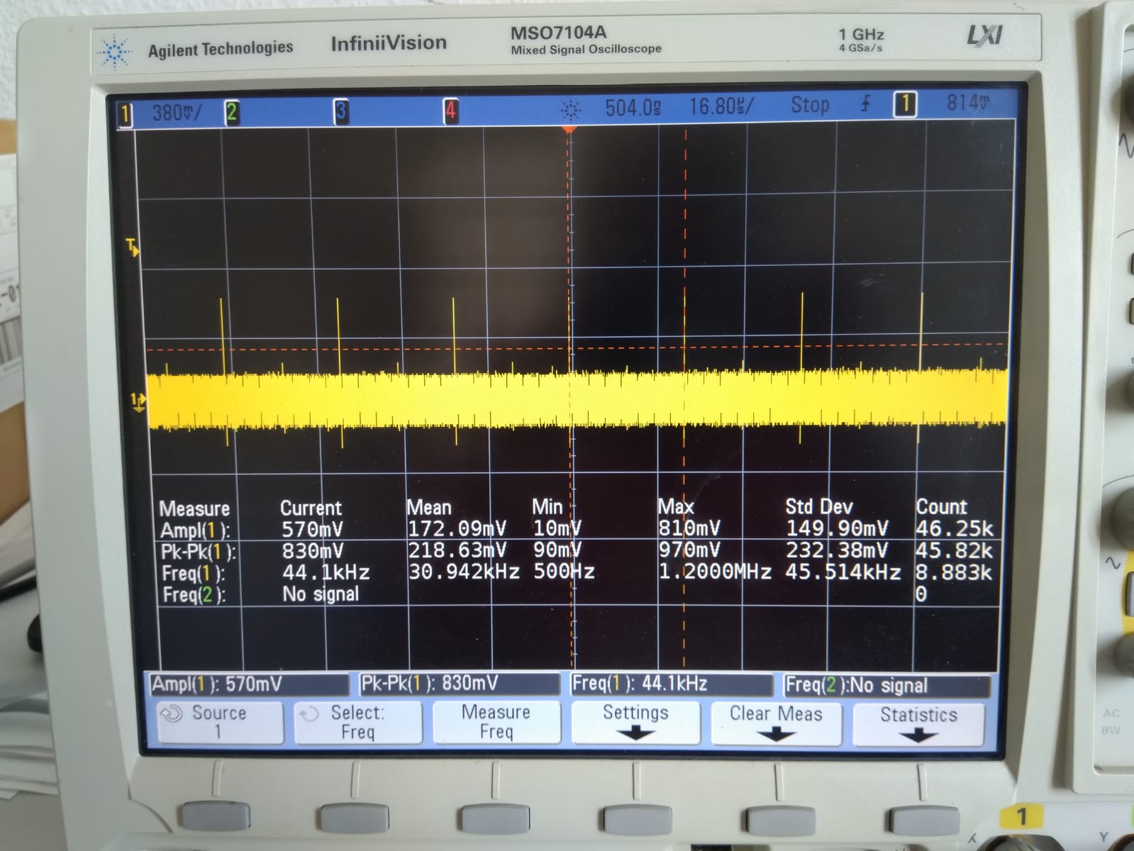
I am not able to get any output.

Problems :

1. not able to write to register 1: (Software Reset), even if I write it as 1, again when I read the value it is 0.

2. is the clock configuration I mentioned above correct? or I need to provide a separate clock for the pll?

CAN ANYONE HELP PLEASE???

  • Hello Rutuja,

    See my answers to your questions below:

    1. Writing 0x01 to register 1 will software reset the device. When you read the register after the reset, it will reset the register to its default value which, in this case, is 0x00. So if you are reading 0x00, that means the software reset was performed.

    2. Configuration you mentioned above sounds correct. 

    Could you please provide a register dump so we can see how you are configuring the device?

    Regards,

    Aaron

  • Aaron Estrada51 said:

    Hello Rutuja,

    See my answers to your questions below:

    1. Writing 0x01 to register 1 will software reset the device. When you read the register after the reset, it will reset the register to its default value which, in this case, is 0x00. So if you are reading 0x00, that means the software reset was performed.

    2. Configuration you mentioned above sounds correct. 

    Could you please provide a register dump so we can see how you are configuring the device?

    Regards,

    Aaron

    Hello Aaron,

    Thank you for your response. I have configured the mentioned registers as follows:

    Registers            Values

    0                      0000 0000

    1                      0000 0001

    4                      0000 0111

    5                      1001 0001

    6                      0000 0100

    7                      0000 0000

    8                      0000 0000

    18                    1000 0001

    19                     1000 0100

    20                      0100 0000

    21                       1011 1100

    27                        0010 0000

    33                        0001 0000

    36                        1100 0000

    38                        0000 0100

    53                        0001 0010

    57                        0000 0000

    61                        0000 0001

    0                          0000 0001

    51                        0000 0000

    52                        1100 0011

    54                         0011 1111

    59                         0000 0000

    60                         0000 0000

    0                            0000 0000

    81                          1000 0010

    82                           0000 1000

    83                            0100 0000

    86                            1000 0000

    I want to have a sampling frequency of 44100.

    So from the i2s I provide the bclk as the pll_clkin of 2.8224Mhz and using the dividers P,R,J and D. I get a pll_clk of 11.2859MHz frequency which I select as the input to the codec_clk. and further selecting the dividers nadc as 1 and madc as 4 and aosr as 64. I get the ADC_fs equal to 44100.

    Here, I would like to make a correction for the value of J in the table number 1, on page no. 22. The given value of J = 32, however according to the formula of fs = (PLLCLK_IN x K x R) / (NADC x MADC x AOSR x P) ON page number 21 of the data sheet, the calculation seem to be incorrect. According to the formula the value of J = 4. (Please correct me if I am wrong)

    I want to use it as single ended. I have kept only the left channel active. and want to use only the IN2L(P) as input.

    Please let me know if I am configuring the device correctly. I Still get no output from the adc.

    Thanks Again!

    Regards,

    Rutuja Salvi

  • Hi Rutuja,

    At first glance, your register config looks correct. Do you have scope shots of your input, CLK signals and DOUT that you can provide?

    As for the possible incorrect calculation, NADC = 8, MADC = 2 and AOSR = 128. With J = 32, R,P = 1 and D = 0, the calculation comes out correct. 

    Regards,

    Aaron

  • Dear Aaron,

    Thank you for you quick response. I am attaching the snapshots of the DOUT, BCLK and WCLK respectively.

    1. DOUT

    2. BCLK

    3. WCLK

  • Hello Aaron,

    I have a couple of questions to ask, 

    1. After configuring the registers one time, should they retain the values that are configured? - because when I write to the registers and read them again they show the default value and not the configured one.

    2. register 36 and 45 are read only registers. if I read them I get values 64(decimal value) and 0  respectively. I am setting the gain to 0dB still it shows the applied gain is not equal to the programmed gain. and the interrupt flag says the left channel signal value is greater the AGC noise. In my perception, it means that the acquired signal power is more than the noise i.e. it detects the signal from the input. (please correct me if I am wrong).

    3. If I provide a sine wave at the input of 1khz, 1Vpp, and try to record... I see something like this on the oscilloscope....why do you thing could this be?

    Also I am attaching a better snapshot of the BCLK(Green) and DOUT(Yellow),

    Thanks and Regards,

    Rutuja Salvi

  • Hi Rutuja,

    Apologies for the slight delay in my response. Please see my responses to your questions below:

    1. The written values should hold. It might be a good idea to double check I2C communication. Also, after your Software reset, you may want to add a small delay if there isn't one already. 

    2. Let me look into this and I will get back to you. 

    3. Where are you measuring this 1 kHz signal? Is it at the DAC output? If so, then what you are seeing is normal and due the the Out of Band noise. 

    Some questions for you:

    1. Are you using an EVM or a personal board?

    2. Your BCLK has large overshoot.What are you using for IOVDD? If you are using IOVDD as 1.8V, you may be violating the abs. max rating for the device.

    Regards,

    Aaron 

  • Aaron Estrada51 said:

    Hi Rutuja,

    Apologies for the slight delay in my response. Please see my responses to your questions below:

    1. The written values should hold. It might be a good idea to double check I2C communication. Also, after your Software reset, you may want to add a small delay if there isn't one already. 

    2. Let me look into this and I will get back to you. 

    3. Where are you measuring this 1 kHz signal? Is it at the DAC output? If so, then what you are seeing is normal and due the the Out of Band noise. 

    Some questions for you:

    1. Are you using an EVM or a personal board?

    2. Your BCLK has large overshoot.What are you using for IOVDD? If you are using IOVDD as 1.8V, you may be violating the abs. max rating for the device.

    Regards,

    Aaron 

    Hello Aaron,

    Sorry for responding late. As per your answers in the previous post :

    1. The first problem detected is the I2C communications. The registers don't hold the written value when read again.

    2. I am waiting for your comments on this

    3. I was measuring the 1Khz signal at the input of the ADC IN2L(P) pin no. 7

    Answer to your questions : 

    1. I am not using the EVM, instead I am using a raspberry pi to do the register configuration.

    2. I am using the IOVDD = 1.8V, since in the datasheet the abs. max values are 1.8V (nominal) and 3.9V(Max). Please correct me wherever I go wrong. 

    This ADC we want to use for an audio project for developing a device in the field of healthcare. First motive is to make this functional

  • Hi Rutuja,

    Since it looks like an I2C communication error, can you send some scope shots of the SCL and SDA lines when sending write/read commands? Also, double check that the address for I2C communication is correct.

    To answer your previous question about register 45, the flag goes high when the AGC algorithm detects that the input signal level is detected below the programmed noise threshold setting. This threshold should be programmed based on the ambient noise expected in the recording environment. 

    Also, the 1kHz input you are seeing on the oscilloscope looks to not be properly triggered or a differential signal. 

    Regards,

    Aaron

  • Hello Aaron and Rutuja,

    I am working with TLV320ADC3100. As well as Rutuja, I am trying to make it functional without success.

    I want to perform a HARDWARE RESET. I noticed that RESET, I2C_ADR0, and I2C_ADR1, when they are without connection (ON THE AIR), its voltage is 1.2 volts.

    QUESTION: On the datasheet, it is NOT mentioned that these pins are configured with internal pull-up resistors.

    For the case of the RESET pin, I tried a solid switch without success. , is there a correct way to control RESET?

    For the case of both I2C_ADRX, if I connect them to ground, from time to time I must switch them with a wire to positive. In other occasions, they are set as negative even if they are without connection (ON THE AIR). , is there a correct way to set or configure I2C_ADRX?

    Regards

     Ivan Maldonado Zambrano

  • Aaron Estrada51 said:

    Hi Rutuja,

    Since it looks like an I2C communication error, can you send some scope shots of the SCL and SDA lines when sending write/read commands? Also, double check that the address for I2C communication is correct.

    To answer your previous question about register 45, the flag goes high when the AGC algorithm detects that the input signal level is detected below the programmed noise threshold setting. This threshold should be programmed based on the ambient noise expected in the recording environment. 

    Also, the 1kHz input you are seeing on the oscilloscope looks to not be properly triggered or a differential signal. 

    Regards,

    Aaron

    Dear Aaron,

    Sorry for the late reply, 

    As per your suggestion I checked the I2C address; I had physically connected the ADR0 AND ADR1 pins to GND earlier.

    which means the address of the device should be 0x18 as given in the datasheet. I tried to read the address with "sudo i2cdetect -y 1" but could not get any address.  

    However, in this condition, I also noticed that even when I am reading from or writing to the registers and print the values, everything works fine. 

    Sometimes I am able to detect the address, sometimes I am not. 

    I have some data from the oscilloscope attached below, when I run my program for reading and writing. I first read the required registers, then I write the values I desire to be in the registers, then I read them back again. As mentioned in earlier posts, when I run the program second time. during the first read section, I see that the values are at the default settings and not the one I wrote. Please let me know if I am going wrong at any step.

    Start, h30 [ h18 | WR ], h00, h00, Stop
    Start, h30 [ h18 | WR ], h04,
    Restart, h31 [ h18 | RD ], h00 NAK, Stop
    Start, h30 [ h18 | WR ], h05,
    Restart, h31 [ h18 | RD ], h11 NAK, Stop
    Start, h30 [ h18 | WR ], h06,
    Restart, h31 [ h18 | RD ], h04 NAK, Stop
    Start, h30 [ h18 | WR ], h07,
    Restart, h31 [ h18 | RD ], h00 NAK, Stop
    Start, h30 [ h18 | WR ], h08,
    Restart, h31 [ h18 | RD ], h00 NAK, Stop
    Start, h30 [ h18 | WR ], h12,
    Restart, h31 [ h18 | RD ], h01 NAK, Stop
    Start, h30 [ h18 | WR ], h13,
    Restart, h31 [ h18 | RD ], h01 NAK, Stop
    Start, h30 [ h18 | WR ], h14,
    Restart, h31 [ h18 | RD ], h80 NAK, Stop
    Start, h30 [ h18 | WR ], h15,
    Restart, h31 [ h18 | RD ], h80 NAK, Stop
    Start, h30 [ h18 | WR ], h1B,
    Restart, h31 [ h18 | RD ], h00 NAK, Stop
    Start, h30 [ h18 | WR ], h21,
    Restart, h31 [ h18 | RD ], h10 NAK, Stop
    Start, h30 [ h18 | WR ], h26,
    Restart, h31 [ h18 | RD ], h02 NAK, Stop
    Start, h30 [ h18 | WR ], h35,
    Restart, h31 [ h18 | RD ], h12 NAK, Stop
    Start, h30 [ h18 | WR ], h39,
    Restart, h31 [ h18 | RD ], h00 NAK, Stop
    Start, h30 [ h18 | WR ], h3D,
    Restart, h31 [ h18 | RD ], h01 NAK, Stop
    Start, h30 [ h18 | WR ], h00, h01, Stop
    Start, h30 [ h18 | WR ], h33,
    Restart, h31 [ h18 | RD ], h00 NAK, Stop
    Start, h30 [ h18 | WR ], h3B,
    Restart, h31 [ h18 | RD ], h80 NAK, Stop
    Start, h30 [ h18 | WR ], h34,
    Restart, h31 [ h18 | RD ], hFF NAK, Stop
    Start, h30 [ h18 | WR ], h36,
    Restart, h31 [ h18 | RD ], h3F NAK, Stop
    Start, h30 [ h18 | WR ], h37,
    Restart, h31 [ h18 | RD ], hFF NAK, Stop
    Start, h30 [ h18 | WR ], h3B,
    Restart, h31 [ h18 | RD ], h80 NAK, Stop
    Start, h30 [ h18 | WR ], h00, h00, Stop
    Start, h30 [ h18 | WR ], h51,
    Restart, h31 [ h18 | RD ], h00 NAK, Stop
    Start, h30 [ h18 | WR ], h52,
    Restart, h31 [ h18 | RD ], h88 NAK, Stop
    Start, h30 [ h18 | WR ], h53,
    Restart, h31 [ h18 | RD ], h00 NAK, Stop
    Start, h30 [ h18 | WR ], h56,
    Restart, h31 [ h18 | RD ], h00 NAK, Stop
    Start, h30 [ h18 | WR ], h00, h00, Stop
    Start, h30 [ h18 | WR ], h04, h07, Stop
    Start, h30 [ h18 | WR ], h05, h91, Stop
    Start, h30 [ h18 | WR ], h06, h04, Stop
    Start, h30 [ h18 | WR ], h07, h00, Stop
    Start, h30 [ h18 | WR ], h08, h00, Stop
    Start, h30 [ h18 | WR ], h12, h81, Stop
    Start, h30 [ h18 | WR ], h13, h84, Stop
    Start, h30 [ h18 | WR ], h14, h40, Stop
    Start, h30 [ h18 | WR ], h15, hBC, Stop
    Start, h30 [ h18 | WR ], h1B, h20, Stop
    Start, h30 [ h18 | WR ], h21, h10, Stop
    Start, h30 [ h18 | WR ], h26, h04, Stop
    Start, h30 [ h18 | WR ], h35, h12, Stop
    Start, h30 [ h18 | WR ], h39, h00, Stop
    Start, h30 [ h18 | WR ], h3D, h01, Stop
    Start, h30 [ h18 | WR ], h00, h01, Stop
    Start, h30 [ h18 | WR ], h33, h00, Stop
    Start, h30 [ h18 | WR ], h3B, h00, Stop
    Start, h30 [ h18 | WR ], h34, hC3, Stop
    Start, h30 [ h18 | WR ], h36, hFF, Stop
    Start, h30 [ h18 | WR ], h37, hC3, Stop
    Start, h30 [ h18 | WR ], h3B, h00, Stop
    Start, h30 [ h18 | WR ], h00, h00, Stop
    Start, h30 [ h18 | WR ], h51, h82, Stop
    Start, h30 [ h18 | WR ], h52, h08, Stop
    Start, h30 [ h18 | WR ], h53, h40, Stop
    Start, h30 [ h18 | WR ], h56, h80, Stop
    Start, h30 [ h18 | WR ], h00, h00, Stop
    Start, h30 [ h18 | WR ], h04,
    Restart, h31 [ h18 | RD ], h07 NAK, Stop
    Start, h30 [ h18 | WR ], h05,
    Restart, h31 [ h18 | RD ], h91 NAK, Stop
    Start, h30 [ h18 | WR ], h06,
    Restart, h31 [ h18 | RD ], h04 NAK, Stop
    Start, h30 [ h18 | WR ], h07,
    Restart, h31 [ h18 | RD ], h00 NAK, Stop
    Start, h30 [ h18 | WR ], h08,
    Restart, h31 [ h18 | RD ], h00 NAK, Stop
    Start, h30 [ h18 | WR ], h12,
    Restart, h31 [ h18 | RD ], h81 NAK, Stop
    Start, h30 [ h18 | WR ], h13,
    Restart, h31 [ h18 | RD ], h84 NAK, Stop
    Start, h30 [ h18 | WR ], h14,
    Restart, h31 [ h18 | RD ], h40 NAK, Stop
    Start, h30 [ h18 | WR ], h15,
    Restart, h31 [ h18 | RD ], hBC NAK, Stop
    Start, h30 [ h18 | WR ], h1B,
    Restart, h31 [ h18 | RD ], h20 NAK, Stop
    Start, h30 [ h18 | WR ], h21,
    Restart, h31 [ h18 | RD ], h10 NAK, Stop
    Start, h30 [ h18 | WR ], h26,
    Restart, h31 [ h18 | RD ], h04 NAK, Stop
    Start, h30 [ h18 | WR ], h35,
    Restart, h31 [ h18 | RD ], h12 NAK, Stop
    Start, h30 [ h18 | WR ], h39,
    Restart, h31 [ h18 | RD ], h00 NAK, Stop
    Start, h30 [ h18 | WR ], h3D,
    Restart, h31 [ h18 | RD ], h01 NAK, Stop
    Start, h30 [ h18 | WR ], h00, h01, Stop
    Start, h30 [ h18 | WR ], h33,
    Restart, h31 [ h18 | RD ], h00 NAK, Stop
    Start, h30 [ h18 | WR ], h3B,
    Restart, h31 [ h18 | RD ], h00 NAK, Stop
    Start, h30 [ h18 | WR ], h34,
    Restart, h31 [ h18 | RD ], hC3 NAK, Stop
    Start, h30 [ h18 | WR ], h36,
    Restart, h31 [ h18 | RD ], hFF NAK, Stop
    Start, h30 [ h18 | WR ], h37,
    Restart, h31 [ h18 | RD ], hC3 NAK, Stop
    Start, h30 [ h18 | WR ], h3B,
    Restart, h31 [ h18 | RD ], h00 NAK, Stop
    Start, h30 [ h18 | WR ], h00, h00, Stop
    Start, h30 [ h18 | WR ], h51,
    Restart, h31 [ h18 | RD ], h82 NAK, Stop
    Start, h30 [ h18 | WR ], h52,
    Restart, h31 [ h18 | RD ], h08 NAK, Stop
    Start, h30 [ h18 | WR ], h53,
    Restart, h31 [ h18 | RD ], h40 NAK, Stop
    Start, h30 [ h18 | WR ], h56,
    Restart, h31 [ h18 | RD ], h80 NAK, Stop

    Many Thanks!

    Best Regards,

    Rutuja

  • Hello Ivan,

    The RESET and ADR0/1 pins do not have internal pull-up resistors and you should add a pull up to IOVDD. Do you have the device powered up correctly when reading the 1.2V?

    Regards,

    Aaron

  • Hi Rutuja,

    I am not sure what you mean by the I2C address being 0x18. If the ADR0 and ADR1 are connected to GND, then the address should be 0x30.

    Regards,

    Aaron

  • Rutuja, 

    Were you able to get this issue resolved?  

    Please let us know if you are still having difficulties

    best regards,

    -Steve Wilson

  • Dear Aaron,

    Extreme apologies for the delayed response. We were talking about 0x18 because as shared in the screenshot, when the I2C_ADR1 and I2C_ADR0 were connected to ground the raspberry pi always detected the I2C address as 0x18 and when I2C_ADR1 was connected to ground and I2C_ADR0 connected to VDD the address was 0x19. Therefore, we never could detect the address as 0x30. Seems like the raspberry pi read the address in other way, because when you read 0011000 consider the I2C_ADR0 pin as LSB, the hex value reading is 0x18. please let us know your comments on this. 

  • Hello Steve Wilson,

    Thank You for your question, we are still stuck with the problem. As discussed with we detect the I2C address as 0x18 on the raspberry pi and not 0x30. We appreciate your comments on this as we are eager to make this work. 

    Thanks in Advance!

    Regards,

    Rutuja Salvi

  • Hello Rutuja,

    My apologies. I misunderstood the I2C address. You are correct that the address should be 0x18 if you are connecting ADR1 and ADR0 to GND. 

    Are you providing a reset after writing to the registers or is there a loss of power somewhere in between? This would cause the registers to reset. Can you provide a schematic?

    Regards,

    Aaron