This thread has been locked.

If you have a related question, please click the "Ask a related question" button in the top right corner. The newly created question will be automatically linked to this question.

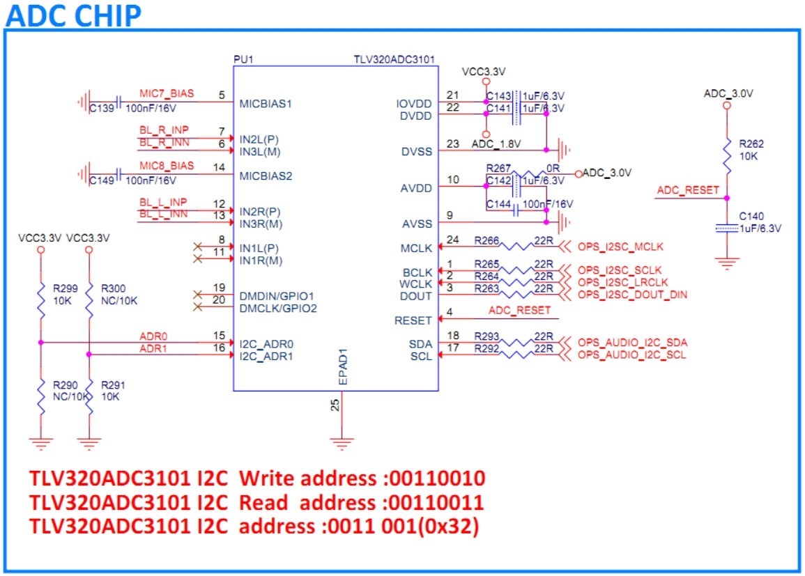
TLV320ADC3101: Could you kindly help to check schematic and the setting for getting sine wave.

Part Number: TLV320ADC3101

Dears:

Could you kindly help to check schematic and the setting for getting sine wave.

delay_ms(100)

write(0x32, [0x00, 0x00])

write(0x32, [0x01, 0x01])

delay_ms(100)

write(0x32, [0x04, 0x00, 0x91, 0x08, 0x07, 0x80])

write(0x32, [0x12, 0x88, 0x82, 0x80])

write(0x32, [0x1B, 0x00])

write(0x32, [0x00, 0x01])

write(0x32, [0x33, 0x00])

write(0x32, [0x36, 0xB3])

write(0x32, [0x39, 0xB3])

write(0x32, [0x34, 0x3F])

write(0x32, [0x37, 0x3F])

write(0x32, [0x3B, 0x20, 0x20])

write(0x32, [0x00, 0x00])

write(0x32, [0x51, 0xC2, 0x00])


  • Lian, 

    for unused Micbias,  just leave the pin floating

    unused inputs can be tied together and terminated with a 0.47uf capacitor to GND. 

    I'm a little confused about your configuration.  The lines below bypass the PGAs,  

    write(0x32, [0x36, 0xB3])

    write(0x32, [0x39, 0xB3])


    but then you also route the signal to the PGAs. and set the gain.  which signal path are you intending to use?


    best regards,

    -STeve Wilson

  • Hi Wilson:

    Thanks for your reply.

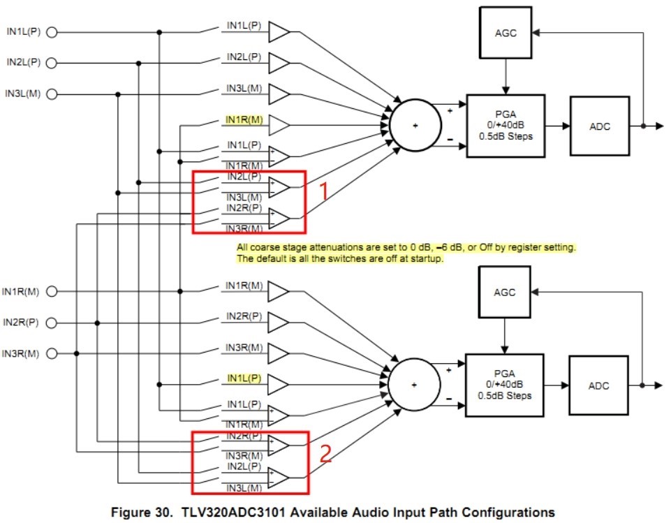
    How can we set the parameters if the signal path as below picture:

  • Luck, 

    it looks like you want to have both differential inputs driving each ADC.  Are you sure you want to have the same inputs to both ADCs? 

    best regards,

    -STeve Wilson

  • Hi Wilson:

    No need to have the same inputs to both ADCs.

    Thanks!

  • Luck, 

    Here is a modified example script from the GUI

    ###############################################

    # Line-In (J9) Stereo Recording

    # ---------------------------------------------

    #

    ###############################################

    ###############################################

    # Software Reset

    ###############################################

    #

    # Select Page 0

    w 30 00 00

    #

    # Initialize the device through software reset

    w 30 01 01

    #

    # Delay 100mS

    d 100

    ###############################################

    ###############################################

    # Clock Settings

    # ---------------------------------------------

    # The codec receives: MCLK = 11.2896 MHz,

    # BCLK = 2.8224 MHz, WCLK = 44.1 kHz

    ###############################################

    #

    # Select Page 0

    w 30 00 00

    #

    # NADC = 1, MADC = 2

    w 30 12 81 82

    #

    # AOSR = 128 (default)

    #

    ###############################################

    ###############################################

    # Audio Settings 

    ###############################################

    #

    # Default Setting: I2S, 16-bits, Slave Mode (BCLK and WCLK are inputs), 3-stating of DOUT disabled

    w 30 1b 00

    ###############################################

    # Signal Processing Settings

    ###############################################

    #

    # Select Page 0

    w 30 00 00

    #

    # Set the ADC Mode to PRB_P1 (default)

    w 30 3d 01

    #

    ###############################################

    ###############################################

    # Recording Setup

    ###############################################

    #

    # Left ADC Vol = 0dB

    w 30 53 00

    #

    # Right ADC Vol = 0dB

    w 30 54 00

    #

    # Select Page 1

    w 30 00 01

    #

    # Mic Bias Powered Down

    w 30 33 00

    #

    # Left ADC Input selection for Left PGA = Differential pair using IN2L(p) and IN3L(M) 

    w 30 34 3f

    #

    # Right ADC Input selection for Right PGA = Differential pair using IN2R(P) and IN3R(M) 

    w 30 37 3f

    #

    # Left Analog PGA Seeting = 0dB

    w 30 3b 00

    #

    # Right Analog PGA Seeting = 0dB

    w 30 3c 00

    #

    # Select Page 0

    w 30 00 00

    #

    # Power-up Left ADC and Right ADC

    w 30 51 c2

    #

    # Unmute Left and Right ADC Channels (Gain = 0dB)

    w 30 52 00

    best regards,

    -Steve Wilson

  • Hi Wilson:

    The wave is as below picture based the setting parameters.

    How can we get good wave? MCLK is 12M, sampling rate is 48K, 16 bits(IIS).

    And other issue is what are the allowable input voltages for PINs like 6, 7, 12 and 13? Do we use differential input, which allows input of - 1.5V ~ + 1.5V voltage?

    Schematic as follows:

  • Luck, 

    is MCLK 12Mhz or 12.288Mhz?  

    regarding input voltages, each pin has an absmax of Vss -0.3V to VDD +0.3V.   

    Full scale input for this ADC is 0.707Vrms single ended or 1.414Vrms for differential.

    best regards,

    -Steve Wilson