This thread has been locked.

If you have a related question, please click the "Ask a related question" button in the top right corner. The newly created question will be automatically linked to this question.

TLV320AIC3104-Q1: the waveform of right output is not good

Part Number: TLV320AIC3104-Q1

Dear team,

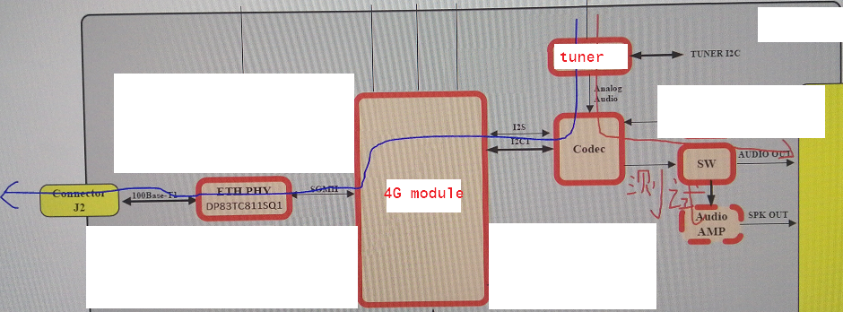
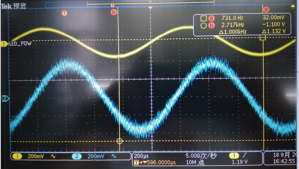
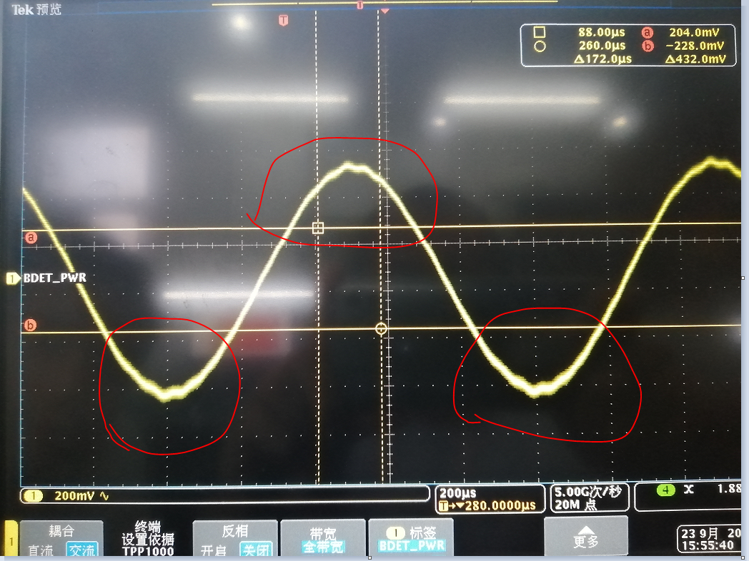
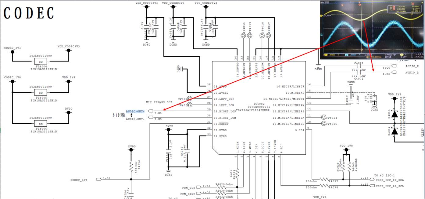
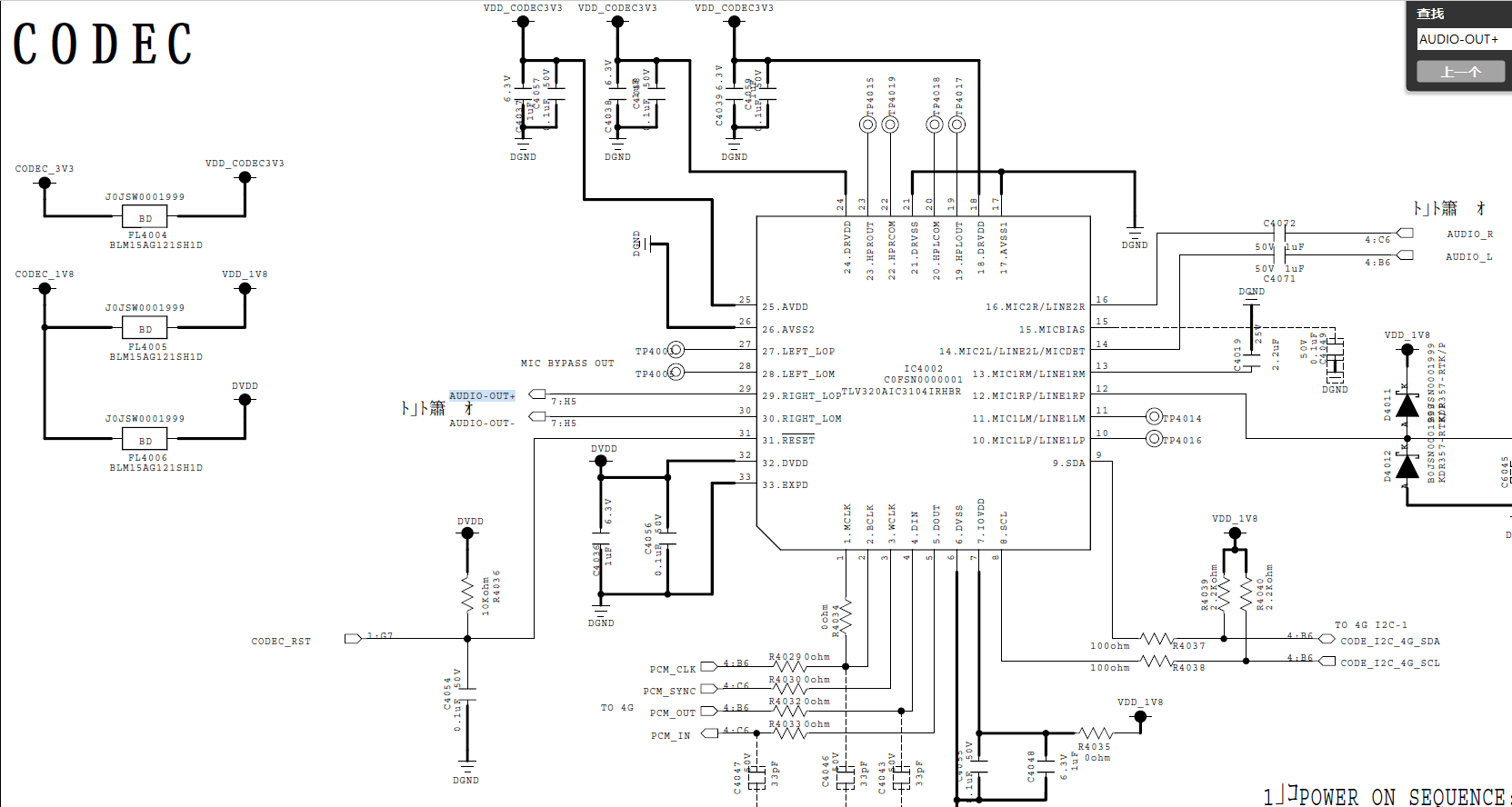
The test found that the input waveform is good (0.05% deviation) but the output waveform is bad (1.2%). Could you please help analyze this problem?

Thanks & Best Regards,

Sherry

  • Hi Sherry,

    This could be caused by out of band noise. A simple low pass filter at the output would help. You can use the EVM schematic in the User's Guide for reference. Also, there is an app note for common noise issues in audio codecs.

    I would also like to recommend tying unused inputs together and connecting them to GND using a .47uF capacitor. Hope this helps!

    Regards,

    Aaron

  • Hi Aaron,

    Thanks for your quick reply! We will try what you recommend.

    Thanks & Best Regards,

    Sherry

  • Hi Aaron,

    When customer adds a RC filter(100ohm&47nF), the output waveform becomes normal. Could you please tell me what does this out of band noise come from? Because they can't add the RC filter now, and the reason is as below,

    The customer's system block is as below, 

    The customer's audio stream(below the blue one) is: codec analog audio input → converted to digital signal by our codec and then output  to 4G module → 4G module transfers the digital audio to the other system (head unit) through the PHY IC. The head unit connected this system via the connect J2 → Head unit's SOC convert digital audio into I2S signal to the DSP, and then the DSP converts the I2S signal into the analog audio output. And the output waveform is bad as the third picture. Therefore they can't add the RC filter at the Head unit side, this project has been finished by other team.

    Now they also test the red line: codec analog audio input → codec analog audio output. And the output waveform is as second  picture(blue waveform).

    1. Now they think maybe the register's configuration is not correct. Could you please provide me an example how to configuration when the condition is as below,

    fS(ref) = 48 kHz, MCLK=2.048Mhz, using the PLL.

    Thanks & Best Regards,

    Sherry

  • Hi Sherry,

    For more info about Out of Band Noise, you can click here to view an app note on this issue.

    To achieve 48 kHz Fs(ref) with an MCLK = 2.048Hz,  the customer can use the example given in section 10.3.3.1 in the data sheet. They will need to program registers 3-6 for PLL and register 7 to set Fs(ref).

    Regards,

    Aaron

  • Hi Aaron,

    Thanks for your reply!

    We didn't find the reason why the output waveform is distorted. Now we have two directions:

    1. check the schematic and layout(I have sent to you by email)

    2. register configuration.

    They use the internal PLL, and the BCLK is the clock source. Their sampling rate is fs=48khz, then the WCLK=48khz, data width=16 bit, so BCLK=2*16*fs=1.536Mhz. fsref has two choices, 48k or 44.1k, and they chose fsref=48khz. Then we can get P=1, R=2, K=32, D=0.

    There is one problem now, when the D=0, PLLCLK_IN has a range: 2M< PLLCLK_IN/P<20M, but according to our configuration, PLLCLK_IN/P=1.536MHz which is beyond the prescribed range. I don't know whether this is related to the distorted output waveform?

    Thanks & Best Regards,

    Sherry

  • Hi Sherry,

    The PLLCLK_IN frequency should always meet the datasheet constraints.

    In this case I do not believe that the PLL settings are responsible,  The LPF needs to be put in place to remove out of band noise going into the amplifier. Especially if the amplifier is a class-D amplifier.  The out of band noise can cause a increase in THD+N after the amplifier.

    please see section 2.4 in this application report

    Can you send over their register configuration?

    best regards,

    -Steve Wilson

  • Hi Wilson,

    Thanks for your reply.

    When they use analog in, analog out, and put RC filter at the output, the output waveform is good without distortion. This also shows that analog in & digital out signal should also be ok, The distortion should comes from other device.

    Thank you!

    Thanks & Best Regards,

    Sherry