This thread has been locked.

If you have a related question, please click the "Ask a related question" button in the top right corner. The newly created question will be automatically linked to this question.

OPA1692: Switching Audio OpAmp In/Out of Circuit

Part Number: OPA1692
Other Parts Discussed in Thread: TINA-TI, LM5165, OPA171, TPS7A47, TPS7A4001

Hello TI Team,

I am currently in the process of trying to bypass the OPA1692 to allow for a passive bypass for a design, however, when switching to the Opamp in or out of circuit the noise floor increases by 1mV. This state can only be exited by removing power to V+ pin and power cycling the Op amp. I have tested the two states the circuit will be in:

1.Powering up the circuit while the audio path is routed through the opamp via SW1.

- Circuit works perfectly. After switching to the bypass path and then switching back to the opamp, the noise is increased.

2.Powering up the circuit in the bypass mode. 

- Bypass works fine but when switching to the opamp the noise is increased.

Please see the circuit being used below:

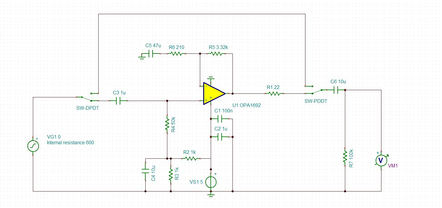
It seems like switching the Opamp in and out of circuit is increasing the noise floor, what is the cause of this and what can be done to correct this? Please let me know if you need any additional information. Thank you very much in advance. 

Best Regards,

Tyler 

  • Hi Tyler,

    Could you please tell us the part# of analog switches on your board, or its electric parameter especially its parasitic caps ?
    I expect it is helpful to break down this issue.

    While, are there any difference of noise between 2 states?
    Once the noise floor was increased, it keeps 1mV(pp or rms?) continuously?

    Finally, if you could see any improvements with modifying the circuit as you can see in the attached TINA-TI file, please let me know.
    OPA1692SW01.TSC

    Best regards,
    Iwata Etsuji

  • Hello Iwata,

    Thank you very much for the quick reply and help! The analog switch being used is actually a 4PDT switch, where two of the poles are being used in the circuit provided. The part number is APEM MMS42, reviewing the datasheet the parasitic capacitance isn't defined. The main callouts in the data sheet are the following:

    -Contact Rating: 100mA at 12VDC

    -Contact Resistance: 20 mOhms

    -Insulation Resistance: 100 MOhm at 500VDC Min.

    The noise between the two states are different. The noise level in the passive bypass is in the noise floor of the audio analyzer around 1uV RMS and the noise through the opamp after the switching the circuit is around 1mV RMS. This noise is broadband noise which spans the entire audio frequency and is constant until the entire unit is power cycled or the power pin is disconnected and reconnected. In addition, the voltage source is a low level audio signal from a transducer with a sensitivity of 1.8mV/Pa.

    Thank you very much for the reference circuit provided. I will test the recommend improvements tomorrow morning when I have access to the audio analyzer. I will follow up tomorrow afternoon with test results.

    Also, I do want to provide some additional information about the voltage source for the circuit. In my reference circuit I designated a 5V voltage source and in your reference circuit you designated a 5V battery. The circuit used in application is being driven from a 5V switching voltage regulator, the LM5165 to be exact. I have attempted to use this voltage regulator in both PFM and COT mode and with different current limiting resistors on the ILIM pin with no change. I see no change in the output voltage, which is regulated at 5V. If needed, I can provide an updated circuit with the LM5165 in the circuit if it is an assumed issue.

    Thank you again. 

    Best Regards,

    Tyler Barkley

  • Hi Tyler,

    Thank you for the information!

    I understood the analog switch on your schematic was just mechanical SW, i.e. only several pF of the parasitic caps are assumed.
    While, do you guess how much parasitic inductance between the voltage source (audio transducer) and the input SW(APEM MMS42)?
    If there were some parasitic inductance, I expected the input shunt resistor on my modified schematic might help to avoid the effect of such parasitic inductance. (On the other hand, I expected the snubber on my modified schematic might help to resolve small oscillation if the switch back action could cause any small oscillation.)

    I would like to do double-check, are you useing a-weighted filter when you test this circuit with the audio analyzer?

    Regarding 5V power supply, I have checked the effect of the ripple noise in the below TINA-TI simulations.

    OPA1692SW03.TSC

    OPA1692SW04.TSC

    OPA1692SW05.TSC

    Is it possible for you to check with clean power supply or the (filtered) buffer for the input common bias circuit such as OPA171 in Fig.63 of OPA1692 data sheet?
    I guess the ripple noise of LM5165 easily couple with the input of OPA1692 via the input common bias circuit.

    Thank you and best regards,
    Iwata Etsuji

  • Hello Iwata,

    Thank you again for your quick reply! I tested your suggestions yesterday and it did not yield any changes in the outcome of the switching. After doing so, I built up the reference circuit I provided on a breadboard and powered it via 4.5V battery supply. When doing so, I did not experience the issue and then I powered my design via the same 4.5V battery supply and the issue again was not present.

    I agree that the ripple of the LM5165 is coupling into the input of the OPA1692, which is undesirable, the thing that still does not make sense is why when powering up with the OPA1692 and using the LM5165 does this issue not present itself? Is it due to the change in load? I have changed the LM5165 into COT mode and PFM, plus adjusted the SS and switching frequency but the issue remains constant. I am starting to think that the LM5165 may not be the best application for this type of project and switching over to a LDO. Do you have any additional suggestions for this setup or possibly a different regulator? The addition of a OPA171 would put the project over on BOM cost and the lack of space for the design does not warrant an additional part.

    Thank you again for all of your help.

    Best Regards,

    Tyler Barkley

  • Hi Tyler,

    Thank you for the confirmation.

    Considering with your test result, I believe the ripple noise of LM5165 should be the root cause of this issue.
    While, I agree it is still unclear how the ripple noise could be coupled around the switch back action.
    I have tried checking any possible coupling path with respect to the considerable parasitic of the schematic.

    OPA1692SW01B.TSC

    However, I have not found any obvious coupling path for this noise issue without the input common bias circuit and V+ pin of OPA1692.
    I just guess that the glitch noise, load transient, or floating node around the switch back action might cause to generate and keep the additional noise coupling path...

    Even if such suggestions are true or false, I would recommend for you to replace LM5165 for OPA1692 supply with a clean power source, considering with your test result.
    When searching LDO for a clean power source, I could see some low noise LDOs; TPS7A47 (up to 36V input and very good PSRR) and TPS7A4001 (up to 100V input and good PSRR).
    I'm sorry I'm not familiar with power management devices, so please post another question on power management forum of E2E if you need further information over the data sheet of LDOs.

    Thank you and best regards,
    Iwata Etsuji

  • Hey Iwata,

    Thank you again for all your help. I'll check out the recommend parts.

    Best Regards,

    Tyler Barkley

  • Hi Tyler,

    Thank you for your considerations!

    If you found similar issue with a clean power supply, please let us know.

    Best regards,
    Iwata Etsuji