This thread has been locked.

If you have a related question, please click the "Ask a related question" button in the top right corner. The newly created question will be automatically linked to this question.

DRV595: DRV595 higher power output

Part Number: DRV595
Other Parts Discussed in Thread: CSD95373AQ5M, CSD

I have been using the DRV595 to drive a TEC with success (4A, 12VDC) however I now need more current (up to 10A).  Is there a higher current version of this IC or alternatively is there a similar driver which I can interface with external mosfets?  Perhaps a monolithic high power H-Bridge IC? Like the DRV595 it would be ideal to drive the differential input single ended and run the driver at a minium of 400kHz in order to keep component size and electrical noise/ripple to a minimum for the TEC.

Is there a reason I cannot use a Synchronous Buck NexFET™ Power Stage (CSD95373AQ5M  or similar) to allow higher currents?  If the PWM outputs from the DRV595 are run via an appropriate resistive network to the PWM inputs on the CSD95373AQ5M  then much higher currents can then be obtained?

Thanks!

http://www.ti.com/lit/ds/symlink/csd95373aq5m.pdf?HQS=TI-null-null-digikeymode-df-pf-null-wwe&ts=1590533123607

  • Hi Chris,

    That's an interesting idea. However, with DRV595, you can change the current continuously, because you have direct control on the output voltage. If a power stage is used here, following the DRV595 output, the problem would be the output voltage across the TEC can only swing between +/-PVDD, is that OK?

    Thanks!

    Regards,

    Sam

  • Hi Sam,

    the output from the DRV595 is a square wave of variable duty cycle between +/-PVDD also with a LC filter smoothing the output across the TEC.  To my mind the output waveform from the power stage will follow the DRV595 output which is connected to the power stage PWM input.  The filter is then placed after the powerstage leading to the TEC as in the original circuit.  How does that sound?

    Regards,

    Chris.


  • Hi Chris,

    OK, I see. 

    One reminder is that you can't use the OUTP to drive a high side secondary FET, and use the OUTN to drive a low side secondary FET. This is because the DRV595 employs BD/1spw modulation, which will have the situation that both OUTP and OUTN equals to PVDD. This will lead to a "shoot-through" on your own power stage.

    Instead, I would recommend you to build a power stage by only using one side PWM output of the amp. For example, use the OUTP. You will have a high side FET driven by OUTP, and insert an inverter to generate the complement driving signal to low side FET. Dead time is also required. 

    By doing this, you will have half gain compared to the differential output. You can set higher gain by changing the configuration on GAIN/SLV pin. 

    Does it make sense?

    Thanks!

    Regards,

    Sam

  • Hi Sam,

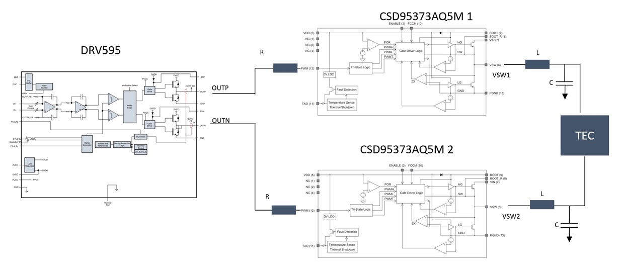
    I think I see but not sure I see why there would be shoot through?  I run the DRV595 in 1spw mode.  My thought was to use two power stages (1 and 2) as power followers for OUTP and OUTN.  Power stage1 input PWM1 is connected to OUTP and powerstage  2 PMW2 input is connected to OUTN. Both OUTP and OUTN have values which swing between power ground and the supply voltage (12VDC) and form positive square waves as the power stage expects to receive.  The power stages respective outputs  VSW1 and VSW 2 should exactly follow their inputs from OUTP and OUTN?

    I'm not sure I see the problem with shoot through because when both OUTP and OUTN are high (PVDD) the output from power stage 1 and 2 (VSW1 and VSW2) will also be PVDD and no current will flow in the load.  Basically OUTP and OUTN waveforms are duplicated by the power stage.  Perhaps I have missed something ?

    Thanks so much for the insights!

    Chris.

  • Hi Chris,

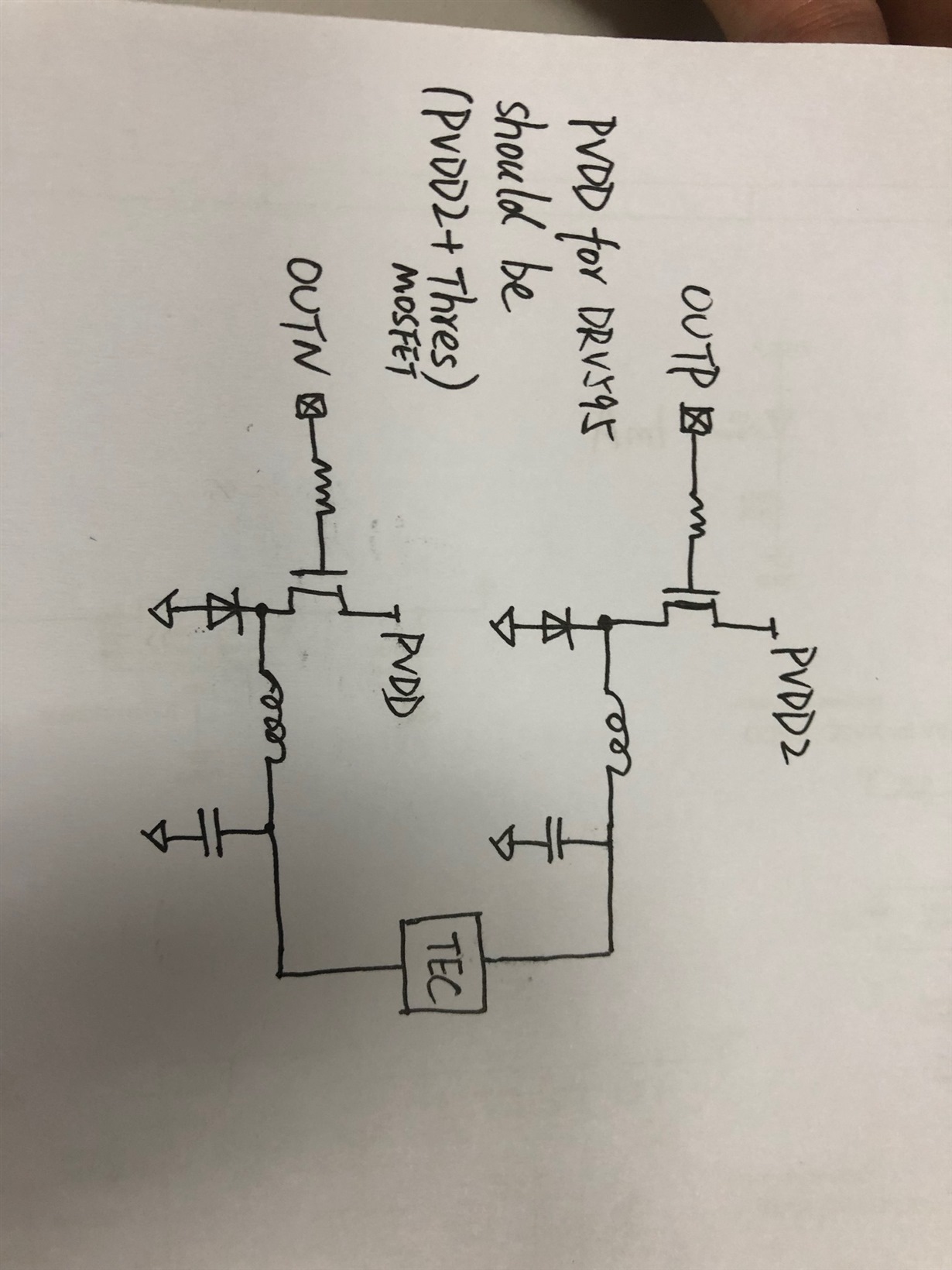
    Sorry I had a wrong picture of your idea... I think now I understand your point. I draw a picture as below, please check if this is your idea.

    Basically I think it's feasible. Some points in my mind,

    1. OUTP/N should be higher voltage than PVDD of the 2nd power stage to make sure the NMOS can be turned on. 

    2. You may need high current capability Schottky  diode, or just put 2 in parallel.

    Any question, please let me know. Thanks!

    Regards,

    Sam

  • Hi Sam,

    thanks so much for your time.  I have made a diagram so it is clearer.  I think it is the same as what you have drawn.  OUTP and OUTN switch between GND and 12VDC (PVDD) for my case so OUTP and OUTN voltages are too high for the CSD95373AQ5M which specifies PWM input range 3.3 V and 5 V PWM Signal Compatible so I would need a resistor divider to scale OUTP and OUTN from 12VDC to ~5VDC ?

  • Hi,

    Yes, that could be a solution. You may also add a zener diode to clamp the PWM input to protect the CSD device.

    As you are actually using an independent power stage IC, it has integrated bootstrap cap, so no need to worry about the NMOS turn-on voltage.

    A soft reminder is that there is a gain on the power stage, which equals to the PVDD of CSD device. 

    Others looks good. Thanks!

    Regards,

    Sam

  • Thanks Sam. The DRV595 and CSD device are both 12V powered so gain should be one. I'll add a 5v zener diode also and try the design. I suppose it can be simulated also. I presume the bootstrap voltage is similar to 16VDC for 12VDC VDD.