This thread has been locked.

If you have a related question, please click the "Ask a related question" button in the top right corner. The newly created question will be automatically linked to this question.

CDCI6214: CDCI6214: Cant get an output signal on Y1 - Y4. Cant get the PLL to lock

Part Number: CDCI6214

Hi,

I am currently trying to configure the CDCI6214 to be implemented in future projects. Even though I did read the given data sheet (rev.B) and forum posts I cant solve my problem.

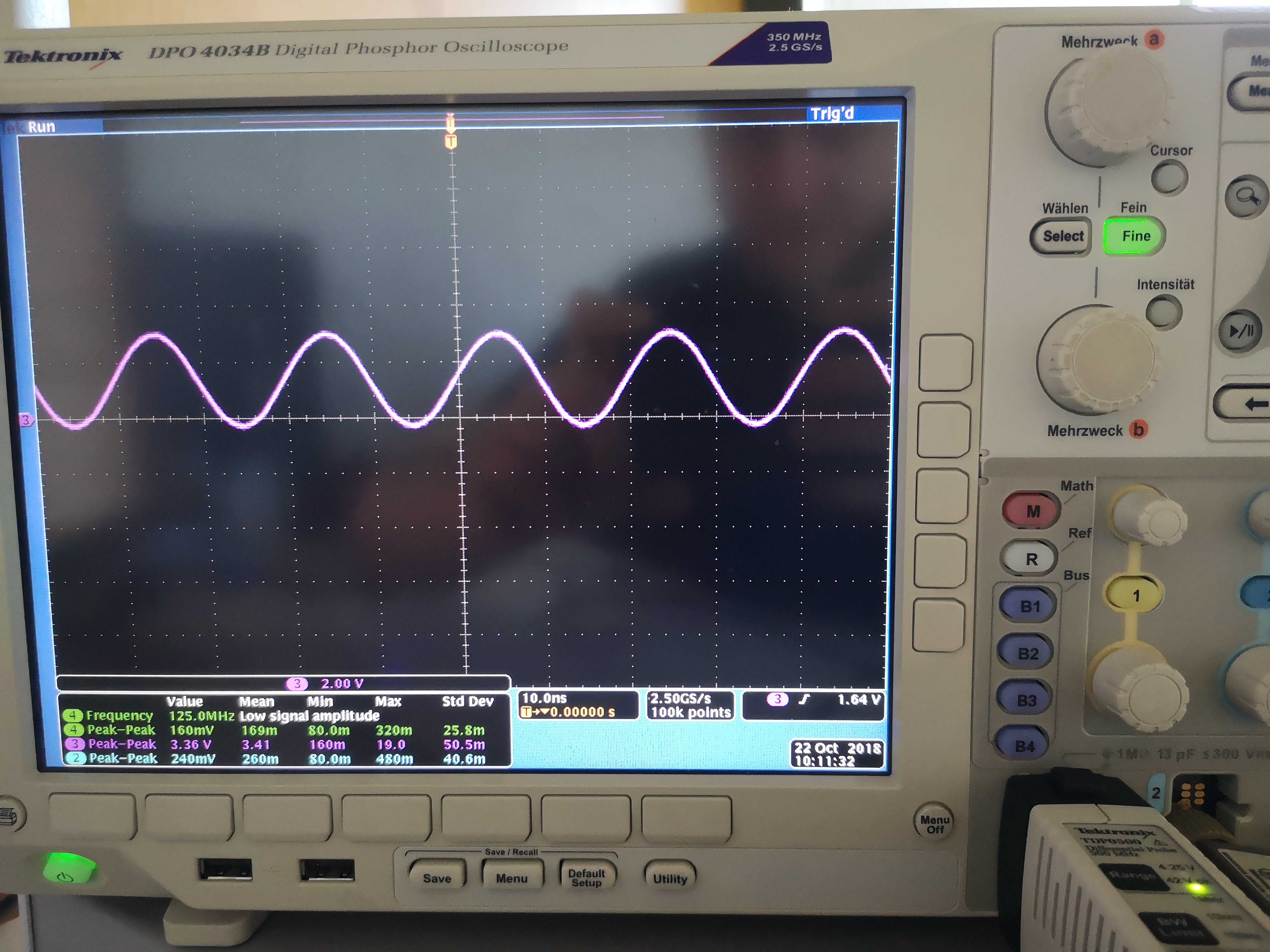
I successfully programmed the device via I2C to produce a bypass-signal through output Y0. But I cant get a output signal on any other output channel. I already tried various different combination.

A STM32 Nucleo L452RE is used for the I2C connection. I am leaving the EEPROMSEL and REFSEL pin floating while selecting the REF-Input via ref_mux. As a input signal I am using a 25Mhz square-wave which is generated with a Arbitrary Generator.
I am using the GPIO1-Pin to check the PLL-lock. Even though I used the values from Table2. (first row) and settings from Figure33. I cant get the PLL to lock.

I transmitted the programming the registers in this order:


Register            Data                Description
_________|________|__________________
0x00,0x0F,0x10,0x37        set ee_lock
0x00,0x28,0x00,0x08       set channel 1 on 1.8V
0x00,0x2E,0x00,0x08       set Channel 2 on 1.8V
0x00,0x34,0x00,0x08       set channel 3 on 1.8V
0x00,0x3A,0x00,0x08       set channel 4 on 1.8V

0x00,0x42,0x02,0x00
0x00,0x3F,0x02,0x10
0x00,0x3E,0x42,0x10
0x00,0x3D,0x15,0x00
0x00,0x3C,0x00,0x18
0x00,0x3B,0x00,0x63
0x00,0x3A,0x00,0x08
0x00,0x39,0x00,0x71
0x00,0x38,0x00,0x04
0x00,0x37,0x00,0x00
0x00,0x36,0x00,0x00
0x00,0x35,0x80,0x00
0x00,0x34,0x00,0x08
0x00,0x33,0x06,0x71
0x00,0x32,0x00,0x04
0x00,0x31,0x00,0x00
0x00,0x30,0x00,0x00
0x00,0x2F,0x80,0x00
0x00,0x2E,0x00,0x08
0x00,0x2D,0x00,0x71
0x00,0x2C,0x00,0x09
0x00,0x2B,0x00,0x00
0x00,0x2A,0x00,0x00
0x00,0x29,0x80,0x00
0x00,0x28,0x00,0x08
0x00,0x27,0x06,0x79
0x00,0x26,0x30,0x09
0x00,0x25,0x00,0x03
0x00,0x24,0x00,0x00
0x00,0x23,0x80,0x00
0x00,0x21,0x00,0x07
0x00,0x1F,0x1E,0x72
0x00,0x1E,0x51,0x40
0x00,0x1D,0x00,0x0C
0x00,0x1C,0x00,0x00
0x00,0x1B,0x0E,0x00
0x00,0x1A,0x0B,0x14
0x00,0x18,0x06,0x01
0x00,0x11,0x06,0xC4
0x00,0x10,0x92,0x1F
0x00,0x0F,0x10,0x37
0x00,0x0E,0x00,0x00
0x00,0x0D,0x00,0x00
0x00,0x0C,0x00,0x00
0x00,0x0B,0x00,0x00
0x00,0x0A,0x00,0x00
0x00,0x09,0x00,0x00
0x00,0x08,0x00,0x00
0x00,0x07,0x00,0x00
0x00,0x06,0x00,0x00
0x00,0x05,0x00,0x00
0x00,0x04,0x00,0x54
0x00,0x03,0x00,0x00
0x00,0x02,0x00,0x30
0x00,0x01,0x6B,0x32
0x00,0x00,0x10,0x40


Also I could not find out which value the "mode"-bit from table19. should have and what it's for.
Further there is a "Recommended Programming Procedure" described in section 8.5.1. It says that you should program the register in descending order from 0x44 to 0x00.
Is this only meant for programming EEPROM because there is no 0x44 register in register maps section 8.6.


Many Thanks
Maximilian Rentschler

  • Hello Maximilian,

    If ch#_sync_delay > 0, then you must have ch#_sync_en = 1 to have the output operate.
    Since ch1_sync_delay = 6 in your configuration, you should change it to 0 or set R38[10] = 0x26[10] = ch1_sync_en = 1.
    Also, I noticed your output divides were set to 0 for ch(2,3,4)_iod_div. So this would power down the output.

    This could address your no output issue. I've not confirmed the PLL lock from EEPROM start at this time.
    Also, did you generate your register map using TICS Pro? In the software you can configure the the device, the save a txt file with all the hex register values. Maybe this will help your situation.

    Please let me know if you still face the PLL unlock issue.

    73,
    Timothy
  • Thank you for the quick answer Timothy,

    I tried the settings that you recommended and still cant get an output signal. I tried enabling the ch1_sync_en as well as disabling it. Also I

    changed all output dividers "ch1/2/3/4_iod_div" to different values. Right now I am only trying to get a output signal through "Y1" that is why the

    other channels where turned off. I also tried routing the BYP-Signal with "ch1_iod_mux" on "Y1" without success.

    I now downloaded the TICS Pro Software for creating the register values but I still cant get the PLL to lock or even a output signal through "Y1".

    These are the values I am currently transmitting:

    R70 0x00460000
    R69 0x00450000
    R68 0x00440000
    R67 0x00430020
    R66 0x00420200
    R65 0x00410F34
    R64 0x0040000D
    R63 0x003F4210
    R62 0x003E4218
    R61 0x003D1500
    R60 0x003C0018
    R59 0x003B1063
    R58 0x003A0008
    R57 0x00398851
    R56 0x00380009
    R55 0x00370000
    R54 0x00360000
    R53 0x00358000
    R52 0x00340008
    R51 0x00338861
    R50 0x00320031
    R49 0x00310000
    R48 0x00300000
    R47 0x002F8000
    R46 0x002E0008
    R45 0x002D0851
    R44 0x002C0011
    R43 0x002B0000
    R42 0x002A0000
    R41 0x00298000
    R40 0x00280008
    R39 0x00270851
    R38 0x00260809
    R37 0x0025C001
    R36 0x00240000
    R35 0x00238000
    R34 0x00220050
    R33 0x00210007
    R32 0x00200000
    R31 0x001F1E72
    R30 0x001E5140
    R29 0x001D000C
    R28 0x001C0000
    R27 0x001B0E00
    R26 0x001A0E01
    R25 0x00192406
    R24 0x00180000
    R23 0x00170000
    R22 0x00160000
    R21 0x00150000
    R20 0x00140001
    R19 0x00130000
    R18 0x0012FFFF
    R17 0x001126C4
    R16 0x0010921F
    R15 0x000F5037
    R14 0x000E0000
    R13 0x000D003F
    R12 0x000C0000
    R11 0x000B003F
    R10 0x000A0000
    R9 0x00090000
    R8 0x00080001
    R7 0x00070C0D
    R6 0x000619CA
    R5 0x00050008
    R4 0x00040000
    R3 0x00031000
    R2 0x00020000
    R1 0x00016B44
    R0 0x00001000


    Thanks a lot
    Maximilian
  • Hello Maximilian,

    I hope to have a more detailed response for you tomorrow. Can you double check your writing with ch1_sync_delay = 0.
    Also, do you have the proper termination for HCSL? Have you tried another output format like LVDS?

    73,
    Timothy
  • Hello Maximilian,

    In review the config you sent I found that...
    * ch1_sync_en = 0, but ch1_sync_delay = 1. This will prevent an output. I changed ch1_sync_delay = 0 to ensure an output.
    * On the EVM PRIREF is configured for AC differential, so I changed ref_inbuf_ctrl from LVCMOS to AC Differential (but it is LVCMOS in dump below)
    * I had to chnage ch1_outbuf_ctrl from HCSL to LVPECL to see an output (but it is HCSL in dump below, provided your output is configured for HCSL, no issue)
    * I had to change ch4_outbuf_ctrl from HCSL to LVPECL to see an output (but it is HCSL in dump below, provided your output is configured for HCSL, no issue)
    * I had to change ch2_iod_div, ch3_iod_div, and ch4_iod_div from 0 to non-zero to see an output... I've set them for the frequencies listed below in the register dump I provide.
    Y0 = 50 MHz from REF
    Y1 = 50 MHz from REF
    Y2 = 75 MHz
    Y3 = 100 MHz
    Y4 = 200 MHz

    With the small variations to the config, I was able to program the EEPROM and have PLL lock all clock outputs operate.
    Confirm an LVCMOS signal to pin 5, REFP.
    - I've provided the register dump below you could program that preserves LVCMOS on inputs and HCSL for output formats on Y1 & Y4.

    It was my observation that without changing the input to AC differential, I was unable to get the PLL to lock. I used a SigGen at 50 MHz and 5 dBm into a balun into SMA_REFP&N.
    > Perhaps there is something with your input causing some grief. Can you measure and show your input waveform?
    > Using AC differential, even when I removed the balun and provided 5 dBm into SMA_REFP single ended, the device still seemed lock and provide output.

    Please try the register dump below and verification of the input. Let me know how it goes.

    73,
    Timothy

    0x00460000
    0x00450000
    0x00440000
    0x00430020
    0x00420200
    0x00410F34
    0x0040000D
    0x003F4210
    0x003E4218
    0x003D1500
    0x003C0018
    0x003B1063
    0x003A0008
    0x00398A51
    0x00380009
    0x00370003
    0x00360000
    0x00358000
    0x00340008
    0x00338861
    0x00320031
    0x00310006
    0x00300000
    0x002F8000
    0x002E0008
    0x002D0A51
    0x002C0011
    0x002B0008
    0x002A0000
    0x00298000
    0x00280008
    0x00270851
    0x00260009
    0x0025C001
    0x00240000
    0x00238000
    0x00220050
    0x00210007
    0x00200000
    0x001F1E72
    0x001E5140
    0x001D000C
    0x001C0000
    0x001B0E00
    0x001A0E01
    0x00190406
    0x00180601
    0x00170580
    0x00160000
    0x00150000
    0x00140001
    0x00130000
    0x0012FFFF
    0x001126C4
    0x0010921F
    0x000FA037
    0x000E0000
    0x000D0000
    0x000C0000
    0x000B0000
    0x000AA4C4
    0x0009A4C4
    0x00080001
    0x00070C0D
    0x0006152C
    0x00050008
    0x00040000
    0x00030000
    0x00020000
    0x00016B44
    0x00001000
  • Hello Timothy,

    thank your for your help. I tried the registers you sent to me but i still cant get an output signal.

    I'm starting to think that there may be some trouble with my test-setup because you said that this register map should run properly. Since I am not using the Evaluation Module but just the chip soldered on a breakout board this could be the only problem left.

    I sent you a picture of the input signal. Its a 50Mhz signal from a SigGen. If you have no further explanation what could cause my problem I will wait till the first prototypes of the project board will arrive to test in on there directly.

    Thank you anyway

    Maximilian

  • Hello Maximilian,

    Maximilian Rentschler said:
    As a input signal I am using a 25Mhz square-wave which is generated with a Arbitrary Generator.

    This was from above...

    Maximilian Rentschler said:
    I sent you a picture of the input signal. Its a 50Mhz signal from a SigGen.

    The prior registers I sent assume 25 MHz input.  If you are using 50 MHz input, then this could be an issue.

    I would boil the troubleshooting down to 4 items.

    1) Ensure you are indeed programming the device.

    If it ever got programmed into a mode where I2C was ignored, the way to get out of this is power up with  EEPROMSEL and REFSEL floating and RESETN/SYNC at VDDREF level.  Sounds like you're probably already doing that, but be sure the RESETN is high.

    Maximilian Rentschler said:
    I am leaving the EEPROMSEL and REFSEL pin floating while selecting the REF-Input via ref_mux

    2) A valid input & input configuration

    Maximilian Rentschler said:
    I sent you a picture of the input signal. Its a 50Mhz signal from a SigGen.

    As for the signal itself, it does appear to meet the requirements for a CMOS in terms of it's amplitude being from ~0 V to ~3.3 V.  Provided you can see the input on Y0, everything should be good.  You might consider testing with ip_byp_mux = 0 for output of REF direct.  If you have a frequency counter synced to your sig gen, this would be the most accurate way to ensure CDCI6214 is getting your input signal properly.

    If any trouble, I would try the AC-differential mode with a smaller swing, ~1.5 Vpp.  Even if you can only provide it to the single input for test purposes.

    Once all inputs considerations are covered, just be sure the output terminations are configured correctly.  For example on our EVM, I had to change to a non-HCSL output to see the clock.

    3) State of the PLL lock.

    You are observing this on the output pin.  You should still be able to get outputs even if it is not locked.  You may need to set cal_mute = 0 to get those outputs.

    A useful method to troubleshoot PLL lock failure is to look at debugging outputs of CLK_PFD_REF (from input) & CLK_PFD_FB (from VCO).  These signals when output from two status pins should be phased locked with respect to one another.  If you're not locked, these outputs should give you clues as to why not.. for example if one frequency is slightly higher or lower, or if a clock isn't present at all.

    * Set GPIO0_OUTPUT_SEL = 0x0a for CLK_PFD_REF and
    * Set GPIO4_OUTPUT_SEL = 0x0b for CLK_PFD_FB

    4) A valid output configuration

    I never did get an explicit response from you to confirm the HCSL was valid for your board, I expect so but am assuming.  You should be able to get outputs (even if PLL is not locked) if the device is configured appropriately.

    --

    Ok, hope this helps, in failing that - the prototypes work for you as expected.  The good news is I'm able to get this working fine on EVM.

    73,
    Timothy