This thread has been locked.

If you have a related question, please click the "Ask a related question" button in the top right corner. The newly created question will be automatically linked to this question.

LMX2594: LMX2594 Spread Spectrum Input Clock

Part Number: LMX2594

Dean,

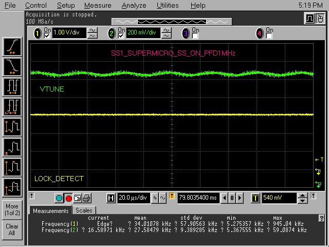
As I have previously posted in this forum, we have been attempting to use the LMX2594 to generate a deterministic, edge-locked 600MHz output clock derived from a 1.2GHz differential clock source.  This source is the standard JEDEC clock provided on a DDR4 (DIMM) socket.  This clock is driven with spread spectrum modulation.  JEDEC specifies a spread-spectrum frequency deviation of 5000 PPM from the fundamental at a modulation period of 30KHz. 

So far, we have not been able to achieve deterministic phase-lock with the LMX2594 in a spread spectrum scenario.  (However, we can achieve phase-frequency lock when spread spectrum is disabled). Since there are other JEDEC-specified devices and FPGAs that employ PLLs that are spread-spectrum tolerant, we were expecting that a device as sophisticated as the LMX2594 would have a similar capability. If not, can TI confirm that the LMX2594 is inherently not compatible with or tolerant of an OSC input clock using spread spectrum modulation as described above? Or conversely, can TI provide us with further guidance as to how the LMX2594 and/or support circuitry be adjusted to meet this design goal?

Thanks,

- Ken

  • Ken,

    So if I understand what you are saying, when the OSCin signal is clean, then there are no issues.

    But when there is spread spectrum modulation on this pin, then the LMX2594 has issues locking.

    If this is the case, I would suspect that the spread spectrum is throwing off the VCO calibration. When the VCO calibrates, it runs off the OSCin clock.  There are three main parts where it chooses the correct VCO core, then VCO capcode, then VCO amplitude calibration.  If the clock is not consistent, perhaps this could confuse the calibration.

    For instance, if you were able to disable the spread spectrum clock in software, then lock the LMX2594, then turn the spread spectrum back on, then I suspect that it would work.

    Another thing that would be useful is to try to make the VCO calibration less sensitive to the calibration.

    Now usually, I would say to increase CAL_CLK_DIV, but you are likely already at the maximum setting for this.  If the part intermittently works, you could consider decreasing the CAL_CLK_DIV bit for diagnostic purposes to see if this agitates the problem.  If so, it points to VCO calibration.

    Also, if the issue is related to VCO calibration, you could do full assist.  In this mode, you read back rb_VCO_SEL, rb_VCO_DACISET, and rb_VCO_CAPCTRL and force these values.  When you read back these values, do it with a clean clock.  Then when you try this with a spread spectrum clock, then force these values as this would get the VCO the correct settings without the need for calibration.

    Regards,

    Dean

  •    Dean,

    We tried both suggestions and another adjustment of our own.

    1.  We SYNCed the clock with no spread spectrum.  PFD = 50mHz and loop current was 15mA.  Lock Detect Duty Cycle was 100% with VTune flat at 1.4V.  Then we enabled spread spectrum.   This immediately  caused the lock duty cycle to reduce from to around 15% with a triangle wave on VTune at a frequency of 32KHz.  No other adjustment we tried would permit SYNCing to the SS clock (~1194MHz to 1200MHz at a modulation frequency of 32KHz).  

    2.  Next, we tried your second suggestion of reading back the rbVCO_DACISET,  rbVCO_CAPCTRL  and rbVCO_SEL when the SS was disabled and the LMX2594 was locked. This yielded:

    R112     rb_VCO_DACISET   ==  0x7000FE

    R111     rb_VCO_CAPCTRL  ==  0x6F001E

    R110     rb_VCO_SEL            ==  06E0448

    After switching SS ON, we wrote the following registers:

    R20  0x149448  (Force ON)

    R20  0x149048  (Force OFF)

    R19  0x13271E

    R16  0x1000FE

    R8    0x086800  (Force ON)

    R8    0x082000  (Force OFF)

    Again, we could not force the output clock to lock to the input clock, although the output frequency was always at or very near 600MHz.

    3.  With SS on and PFD = 50MHz, loop filter current at 15mA, lock detect at 15% duty cycle and VTune a triangle wave at 32KHz, we starting reducing the PFD from 50 MHz down to the minimum allowed at 1MHz.  We noticed as the PFD frequency got lower, the lock detect duty cycle increased and the VTune amplitude reduced, centered around the 1.4V average we noted when in lock.  At 1MHz, the duty cycle was back at 100% and Vtune was nearly flat.  Still no phase lock, however.  I have attached a few samples of these waveforms.

    We were wondering if it would be useful to make adjustments to both the loop filter components and the PFD frequency that would allow both phase and frequency lock in our SS environment?

    Please advise.  Thanks again,

    - Ken

  • Ken,

    A few things:

    As for the writing, what you want to ensure no VCO calibration issues:
    1. Lock PLL with clean reference
    2. Read back rb_VCO_DACISET, rb_VCO_SEL, rb_VCO_CAPCTRL
    3. Write VCO_DACISET as rb_VCO_DACISET, VCO_SEL as rb_VCO_SEL, and VCO_CAPCTRL as rb_VCO_CAPCTRL.
    4. Set VCO_CAPCTRL_FORCE=VCO_DACISET_FORCE=VCO_SEL_FORCE=1 and KEEP these as one, don't change back to 0.
    5. Enable spread spectrum.


    But your issues go farther than this because I think that your spread spectrum is too broadband. Realize that there are 7 VCO cores and each VCO core has 183 different frequency bands. So suppose you are at 8 GHz and locked to a 100 MHz reference. Now lets say that the VCO can tune in the ballpark of +/- 80 MHz without changing the VCO_CAPCTRL (i.e. no calibration). Now suppose your spread spectrum is FM modulation that goes from 99.9 to 100.1 MHz. Then at the output the VCO would want to try to go from 7992 to 8008 MHz, so this is within the 80 MHz range, but just to make you aware of this.

    Now another consideration is the loop bandwidth. If you reduce this, it supresses the spread spectrum modulation. The right way to do this is redesign the filter for a narrow loop bandwidth. But the less optimal way to do this is reduce the phase detector frequency or the charge pump gain. The fact that reducing these seems to help makes me think that you just need a narrower loop bandwidth to supress all this modulation.

    Regards,
    Dean
  • Dean,

    As you indicated, we were able to reduce the amplitude of the VTune triangle wave even further by reducing the charge pump gain. I am motivated to do it the right way and redesign the filter for a narrow loop bandwidth. To that end, I have downloaded the PLLatinum Sim tool. However, I could use some help in selecting the design targets for this tool. Some seem straightforward. For example, given the input clock spread spectrum deviation range of 1.194GHz to 1.200GHz the VCO range would be 9.552 GHz to 9.600 GHz which should indicate VCO2 as the VCO core.

    Since we were not able to lock with the PFD frequency set to the TICsPro minimum of 1MHz , are you suggesting that we need to use the loop filter to narrow the bandwidth even further? If so, how much more should we narrow this parameter? Does the spread spectrum modulation period of 32KHz have a direct impact on the loop filter bandwidth choice?

    Should we stick with the 3rd order filter configuration per the EVM reference design or would a simpler 2nd order filter suffice? I notice that whether I choose 2nd or 3rd order and then select Calculate Loop Filter, the tool selects one of the caps as 1.5nF and then issues a warning that this device should be greater than 3.3nF. Do I delete this cap?

    This rookie can sure use your help. Please advise.

    Thanks,

    - Ken
  • 1004.LMX2594 Minimum High Order Cap for Vtune.pdfKen,

    For starters, I would try a 2nd order loop filter.  I think that the loop bandwidth should be narrow enough to supress the modulation.  Also, it is more stable and resistant to tweaking the gain of the charge pump and phase detector frequency

    PLLatinum Sim defaults a wide loop bandwidth for optimal jitter, but this assumes that you have a clean reference, which you definitely do not.  I would target a much narrower loop bandwidth, probably something in the 10 kHz range, but I'm not exactly sure.

    The warning about the cap is related to the fact that the VCO phase noise is degraded if the AC impedance in the 100 kHz - 10 MHz range is too low as seen looking out from the Vtune pin.  This becomes an issue with wider loop badnwidth filters, but for your filter, you should have no problem as the loop bandwidth should be much narrower and naturally this capacitor woudl be larger.  If you choose a 2nd order loop filter, then the capacitor C1 is the critical one.   I have attached a report that gives more details about this minimum capaticance.

    Regards,

    Dean

  • Dean,

    As a sanity check, I compared the results against the 3rd order loop filter design with FPD=200MHz, Kpd=12mA and loop filter bandwidth of  ~286KHz as shown in Figure 51, Page 59 of the LMX2594 datasheet (which is the loop filter configuration we are currently using).  The calculator did not produce the same component results as shown in the datasheet/EVM calculation including a loop bandwidth of only 164.5KHz..  Am I missing some other critical variables in this calculation?   My results are attached as EVM_Filter.jpg.  

    I also attempted a  2nd order loop filter design based on FPD=50MHz, Kpd=15mA and loop filter bandwidth of ~10KHz.     Since you mentioned that C1 was key for this design, I was concerned about the relatively high values of C1 and C2 as compared with the original EVM design.  Are these reasonable component values to implement a 10KHz loop bandwidth as you suggested?  These results are attached as SS1_Filter.jpg.

    Sorry I had to use .jpg files.  The forum wouldn't accept the much smaller .sim files.

    Thanks,

    - Ken

  • Ken,

    The second order loop filter looks like a reasonable one.

    As for the design not matching, realize that a 3rd order filter has 5 components, and therefore needs 5 constraints, which typically are:
    loop bandwidth, phase margin, gamma, T3/T1 ratio, and maximizing the value of C3.
    Furthermore if the VCO gain, VCO frequency, charge pump gain, or phase detector frequency changes, it changes the components.

    Regards,
    Dean
  • Dean,
    I tried 5 different 2nd order filters with bandwidths of 200KHz, 100KHz, 50KHz, 20KHz and 10KHz. All SYNCed with SSC turned off. All failed to SYNC with SSC turned on. In each case I ran the PFD from 50MHz down to 1MHz with improvement on VTune and Lock Detect as I reduced the PFD and Gain. With the 10kHz BW filter, PFD= 1MHz and Gain = 6mA, the Lock Detect duty cycle was 100% and VTune was flat with no detectable trace of the 32KHz triangle waveform. I am prepared to order some bigger caps and reduce the loop filter bandwidth even further if you think it is worth the effort. Is there anything else that I can try to force a spread spectrum SYNC? By the way, was your suggestion of setting the loop bandwidth down to 10KHz based on the spread spectrum deviation or some other factor?

    Thanks,

    - Ken
  • Ken,

    In regards to choosing loop bandwidth based on FM deviation, I was thinking more based on FM modulation rate ...

    Conisider FM modulation with frequency deviation of Fdev and modulation frequency of Fmod. The spur offset frequency is Fmod and the spur level before accounting for shaping of the loop filter response is 20*log(B/2) where B=Fdev/Fmod.

    Now if we assume spread spectrum is periodic, then we can write a Fourier series representation and consider it to be the sum of many FM modulation waveforms. Now if the loop bandwidth will cut off any elements in the modulation that is wider than Fmod. Fdev is not the offset, but rather the magnitude of the modulation.

    In regards to the SYNC not working ...

    It sounds like it does work with no spread spectrum.

    It sounds like if you try to SYNC with spread spectrum running, it doesn't work. Because the SYNC is reclocked through the Fosc signal, this sounds believable. I think that this might just be the way it is.

    However, have you tried to first do the SYNC with spread spectrum off, and then turn on the spread spectrum after SYNC? If the spread spectrum for all inputs is the same and phase coherent, I would think it could maintain phase SYNC.

    Regards,
    Dean
  • MY REPLY:

    Dean,

    In your equation, you do not define B. Is B = loop bandwidth?

    Fdev = 5000(ppm)/1000000 * 1.2GHz = 6MHz and
    Fmod = 32KHz

    Then B = 6MHz / 32Khz = 187.5 Hz.

    Spur level = 20*log(187.5 / 2) = 39.4 (Hz?)

    My Fourier series theory has gotten a bit stale. Are you suggesting reducing the loop bandwidth to < 187.5 Hz? Also how do I use the spur offset?

    We have tried a variation of your second suggestion. We lock with the platform in SSC_OFF. Then we reboot the platform with continuous power on the LMX2594 and its supporting components. During the reboot, we have the opportunity to enable SSC through the system BIOS. Even though the OSC clock turns OFF before re-enabling it with SSC ON, we observe that the LMX2594 output clock maintains its 600MHz during this interval. When the SSC=ON clock is re-established, the SYNC condition is lost. Unfortunately, the bios and motherboard vendors do not support real-time switching of SSC ON/OFF capability.

    Please advise. Thanks,

    - Ken
  • Ken,

    B was the modulation index for FM modulation. B = Fdev/Fmod., spur = 20*log(B/2) As B is the ratio of two frequencies, it is a dimmensionless quantity, not does NOT have units of Hz. However, this formula assumes narrowband FM where B<<1, which is not the case here. Technically, the spur is really given by 20*log(J0(B)) where J0 is the Bessel function of the first kind. Only if B<<1 can the previous formula be used.

    Reducing the loop bandwidth more reduces the modulation that passes through.So in the case you have here, think of your modulation as a continium of spurs. Now if you had loop bandwidth of 10 kHz, then all modulation above 10 kHz is attenuated and the modulation below passes through.

    However, in regards to the SYNC function, it seems harder to do in your setup. If you the OSCin clock, then you lose phase lock. Now at the VCO, there are 7 cores of 183 capcodes each. These frequency bands are on the order of +/- 50 MHz, but then you dovide down by a factor of about 16. So in other words, if you remove the input reference after you lock, your output frequency might only move on the order of 4 MHz, but the PLL is still unlocked.

    Regards,
    Dean
  • Dean,
    Is it fair to say that we've exhausted all of our options by adjusting the Fpd, charge pump gain and loop bandwidth to acquire PLL lock in SSC mode? If so, what mechanism in the PLL would allow it to track the SSC modulation if we could instantaneously switch from SSC_OFF to SSC_ON without temporarily disabling the input clock? Wouldn't this eventually drive the PLL out of lock anyway? Unless you have some other insights as to what we might try, I'll have to assume that we only have a solution with the LMX2594 if the application can be run in a non-SSC implementation.
    Do you concur?
    Thanks,
    - Ken
  • Ken,

    We have 3 issues we are talking about, so I'm losing track, but here's what I remember.

    1. Lock detect erroneously reports unlock/non-100% duty cycle when PLL is actually in lock. In other words, PLL perceives itself to be out of lock
    Now this issue is impacted by Fpd and charge pump gain and can be dealt with. Reducing phase detector frequency reduces sensitivity of the lock detecct.

    2. PLL truely doesn't lock in SSC mode
    I can't remember all the conversation, but if you try to calibrate the VCO with SSC on, this might causes issues. The input reference drives the VCO calibration that counts on this frequency being correct. If this frequency is off, the VCO will calibrate to the wrong band and even if the clock comes back, it is stuck in the wrong band. There are 7 VCO cores with 183 bands each for 7 x 183 = 1281 frequency bands. Also, if the frequency is varying during the VCO calibration process (triggered by writing FCAL_EN=1 to register R0), then maybe this is what is causing the issue.

    3. If I give a reference in SSC mode to two locked LMX2594's, it doesn't keep both in SYNC
    I though that there were some discussions on this, but I'm not sure if there is anything that can be done about this.


    So the SSC is indeed problematic if it is running all the time. I was thinking if you could just get hte PLL calibration to run without the SSC. Or another option is you can try full assist. For this, you lock the PLL without SSC and then read back rb_VCO_SEL, rb_VCO_CAPCTRL, and rb_VCO_DACISET. Then you just force these values and there is no way for the calibration to be confused.

    Regards,
    Dean