This thread has been locked.

If you have a related question, please click the "Ask a related question" button in the top right corner. The newly created question will be automatically linked to this question.

LMK04828 Not Responding to SPI

Other Parts Discussed in Thread: LMK04828

Hi,

We are interfacing LMK04828 with ZCU102 reference board. Setting SPI Mode 0 (CPOL=0, CPHA=0). 

We are Using 3-Wire mode and the CS#,SCLK and SDIO pins are probed using Oscilloscope and obtained correct Waveforms.

ie., the 24-bit commands for LMK04828 are reaching the pins. But No response is received from the LMK04828.

We measured the voltages at LDObyp1~2.5V, LDObyp2~1.5V and OSCin and CLKin~1.6V.

Please Help us Here.

  • Also Please help me to find on which pin I can read back the Register values
  • Hello Nikhil,

    Any chance your RESET pin 5 is held high?

    Please see the attached file on the readback pins.  Note, on POR, 3-wire SPI readback mode is enabled with an open drain output.

    73,
    Timothy

    SPI Readback on LMK0482x Family.pdf

  • Hi Timothy,

    Thank you very much for the response and also for the document.

    RESET(pin5) is pulled down and also probed correctly as low.

    We are using EMIO Pins of ZCU102 Board for SPI Programming and Please find our programming sequence below. Please verify and give your valuable comments:

    #include <stdio.h>
    #include <stdlib.h>
    #include <stdint.h>
    #include <unistd.h>
    #include <fcntl.h>
    #include <linux/types.h>
    #include <linux/spi/spidev.h>

    #define RESET_CMD 0x000080
    #define NORMAL 0x000010
    #define DCKOD 0x010010
    #define DCKOB 0x010302
    #define DCKFMT 0x010701
    #define VCOMX 0x013800
    #define FIXED1 0x01457F

    #define CLKINEN 0x01461A
    #define CLKINS 0x01471A
    #define CLKINS1 0x014802
    #define CLKINS2 0x014942
    #define PLL1N1 0x01533D
    #define PLL1N2 0x015409
    #define PLL1CP 0x015BDF
    #define PLL2R1 0x016000
    #define PLL2R2 0x016102
    #define PLL2PRE 0x016269
    #define FIXED2 0x0171AA
    #define FIXED3 0x017202
    #define FIXED4 0x017C15
    #define FIXED5 0x017D33
    #define PLL2N1 0x016600
    #define PLL2N2 0x016700
    #define PLL2N3 0x01680B
    #define PLL2CP 0x016959
    #define LP2R4R3 0x016C00
    #define LP2C4C3 0x016D00

    int load_config(unsigned int cmd, int fd)
    {
    int ret;
    uint8_t RecvBuf;
    ret = write(fd,&cmd,6);
    if (ret < 0)
    {
    printf("error writing data \n");
    exit (0);
    }
    /*ret = read(fd,&RecvBuf,3);
    if(ret < 0)
    {
    printf("error reading data \n");
    exit(0);
    }
    printf("Received Value: %d\n",RecvBuf);
    return RecvBuf;*/
    return 0;
    }

    int readback(unsigned int cmd, int fd)
    {
    int ret;
    uint8_t RecvBuf;
    ret = write(fd,&cmd,2);
    if (ret < 0)
    {
    printf("error writing data \n");
    exit (0);
    }
    ret = read(fd,&RecvBuf,1);
    if(ret < 0)
    {
    printf("error reading data \n");
    exit(0);
    }
    printf("Received Value: %x\n",RecvBuf);
    //return RecvBuf;
    return 0;
    }

    int main(int argc, char **argv)
    {
    printf("Hello World!\n");
    int stop=0;
    int fd,ret;
    int fch=1;
    fd = open("/dev/spidev1.0",O_RDWR);
    if (fd < 0)
    {
    printf("error opening node \n");
    exit (0);
    }
    else
    {
    do
    {
    printf("Specify the Output Frequency: (1->161Mhz 2->156Mhz 3->195MHz 4->257MHz 5->Read Back 6->Stop 7->Iverase Read Back: \n");
    scanf("%d",&fch);
    switch(fch) {

    case 1:
    printf("Output Frequency: 161.1328125Mhz\n");
    load_config(RESET_CMD,fd);
    load_config(NORMAL,fd);
    load_config(DCKOD,fd);
    load_config(DCKOB,fd);
    load_config(DCKFMT,fd);
    load_config(VCOMX,fd);
    load_config(FIXED1,fd);
    load_config(0x014A33,fd);
    load_config(CLKINEN,fd);
    load_config(CLKINS,fd);
    load_config(CLKINS1,fd);
    load_config(CLKINS2,fd);
    load_config(PLL1N1,fd);
    load_config(PLL1N2,fd);
    load_config(PLL1CP,fd);
    load_config(PLL2R1,fd);
    load_config(PLL2R2,fd);
    load_config(PLL2PRE,fd);
    load_config(FIXED2,fd);
    load_config(FIXED3,fd);
    load_config(FIXED4,fd);
    load_config(FIXED5,fd);
    load_config(PLL2N1,fd);
    load_config(PLL2N2,fd);
    load_config(PLL2N3,fd);
    load_config(PLL2CP,fd);
    load_config(LP2R4R3,fd);
    load_config(LP2C4C3,fd);
    printf("Write Completed\n");
    break;
    case 2:
    printf("Output Frequency: 156.25Mhz\n");
    break;
    case 3:
    printf("Output Frequency: 195.3125Mhz\n");
    break;
    case 4:
    printf("Output Frequency: 257.8125Mhz\n");
    break;
    case 5:
    printf("Readback\n");
    load_config(0x000080,fd);
    load_config(0x000010,fd);
    load_config(0x01457F,fd);
    load_config(0x014A33,fd);
    load_config(0x0171AA,fd);
    load_config(0x017202,fd);
    load_config(0x017C15,fd);
    load_config(0x017D33,fd);

    load_config(0x014833,fd);
    load_config(0x014973,fd);
    load_config(0x015F3B,fd);
    load_config(0x016E3B,fd);

    readback(0x8003,fd);
    break;
    case 7:
    load_config(0x800000,fd);
    load_config(0x100000,fd);
    load_config(0x7F4501,fd);
    load_config(0x334A01,fd);
    load_config(0xAA7110,fd);
    load_config(0x027201,fd);
    load_config(0x157C01,fd);
    load_config(0x337D01,fd);

    load_config(0x334801,fd);
    load_config(0x734901,fd);
    load_config(0x3B5F01,fd);
    load_config(0x3B6E01,fd);

    readback(0x0380,fd);
    break;
    case 6:
    stop=1;
    break;
    default:
    printf("Choose a Valid Option\n");
    }
    }while(stop==0);

    }

    return 0;
    }

  • Hi Timothy,

    Good news, I could communicate with LMK04828 through SPI and I can Write the registers and also read what I write through 4-wire mode.

    I am using a custom Board. Using the parameters as below:

    Oscin : 156.25Mhz

    CLKin: 30.72MHz

    I am expecting 156.25MHz LVDS output through DCLKOUT1

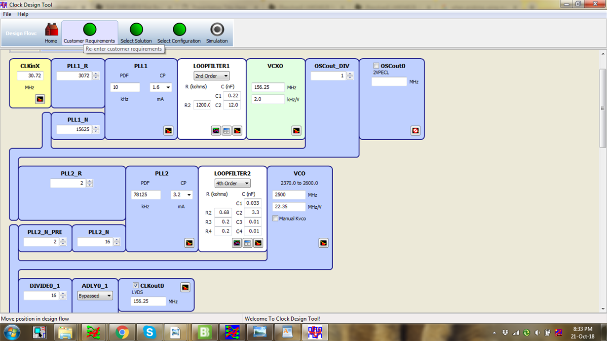
    Also attaching the Clock design tool output for my configurations.

    Please Help to get possible register configurations for this if you have any or please suggest which all registers are need to be taken care.

    Thanks in Advance

    Nikhil Krishnan R

  • Hi

    Please find our register set values below:

    0x100 -> 0x10
    0x103 -> 0x02
    0x106 -> 0x71
    0x107 -> 0x01
    0x138 -> 0x01
    0x146 -> 0x1A
    0x147 -> 0x1A
    0x148 -> 0x03
    0x149 -> 0x43
    0x150 -> 0x43
    0x155 -> 0x0C
    0x156 -> 0x00
    0x159 -> 0x3D
    0x15A -> 0x09
    0x160 -> 0x00
    0x161 -> 0x02
    0x162 -> 0x49
    0x166 -> 0x00
    0x167 -> 0x00
    0x168 -> 0x10
    0x169 -> 0x59
    0x16C -> 0x00
    0x16D -> 0x00

    All other registers are with default value

    Please verify and suggest changes.
    Please help me, this is something urgent.
  • Hello Nikhil,

    In your registers, with 0x16249 you are programming PLL2_REF2X_EN = 1, you have PLL2_R = /2 and PLL2_N = /16, this results in a VCO frequency of 5000 MHz, you want 2500 MHz, I suggest you turn the doubler off (0x162 --> 48) to get the 78.125 MHz phase detector frequency.

    Also, as per 9.5.1 on page 49 of datasheet.
    Program 0x000 --> 0x80

    And also, Add registers before 0x166:
    0x145 --> 0x7f
    0x171 --> 0xaa
    0x172 --> 0x02
    0x17c --> 0x15
    0x17d --> 0x33

    Also, your PLL1 R divider (CLKin1_R) is 3072. You have a 30.72 MHz frequency. This results in a very low PLL1 phase detector frequency. I suggest increasing the PLL1 charge pump (as is the case in the CDT sim), set 1550 uA with 0x15b --> 0xdf.

    Just confirming you do have a 3.3 V DC coupled CMOS signal into CLKin1, otherwise I would suggest using the CLKin1_TYPE = Bipolar.

    73,
    Timothy

  • Hi Timothy,

    Very glad to say that we got the output frequency well.

    Initial Programming sequence was done as per the datasheet.

    Problem was with Frequency Doubler and Charge pump gain. We gave the register values as suggested and got the output.

    Our input is 3.3VDC CMOS signal to CLKIN1 and got LVDS output at DCLKOUT1.

    Is there any register to be configured to increase the stability of the output frequency?

  • Hello Nikhil,

    Do you see some slight shifting of the frequency at a 10 kHz rate?  The phase detector of 10 kHz is low, so if the VCXO you are using has some leakage, it could cause the frequency to drift slightly before the next turn-on of the charge pump which would correct the frequency.  This would also be seen as a 10 kHz spur.  Although narrow loop bandwidths would result in attenuation of this spur.

    Things you could try:

    • Designing a narrower loop filter could help.
    • A VCXO with higher input impedance could help.
    • Using an active loop filter with op-amp or op amp configured as unity gain buffer would allow the input impedance of an opamp to replace the input impedance of the VCXO.  This could also help.

    73,
    Timothy